STI pull-down to control SiGe facet growth

a technology of sige facet and pull-down, which is applied in the direction of transistors, semiconductor devices, electrical equipment, etc., can solve the problems of increasing parasitic current leakage, and achieve the effect of reducing dislocations

Inactive Publication Date: 2005-08-30
GLOBALFOUNDRIES INC
View PDF32 Cites 16 Cited by
  • Summary
  • Abstract
  • Description
  • Claims
  • Application Information

AI Technical Summary

Benefits of technology

[0007]One object of the present invention is to provide a method of fabricating a SiGe heterojunction bipolar transistor wherein the SiGe base resistance is reduced.
[0009]A further object of the present invention is to provide a method of fabricating a SiGe heterojunction bipolar transistor in which diminished parasitic current leakage is achieved.
[0014](c) forming a SiGe layer on the upper surface of the semiconductor substrate as well as the recessed isolation surface, wherein said recessing controls facet growth at edges of the SiGe layer thereby reducing dislocations therein.

Problems solved by technology

A major problem with prior art SiGe heterojunction bipolar transistors of the type illustrated in FIG. 1 is that during the deposition of the SiGe layer, facet regions (labeled as 30 in FIG. 1) grow at the edges of the SiGe layer between the polycrystalline Si region and the SiGe base region.
The growth of facets near the this corner leads to increased parasitic current leakage as well as shorts which are caused by the presence of excessive dislocations in the structure.

Method used


Image

  • STI pull-down to control SiGe facet growth
  • STI pull-down to control SiGe facet growth
  • STI pull-down to control SiGe facet growth

Examples


Embodiment Construction

[0028]The present invention which provides a method for improving the SiGe bipolar yield of a SiGe bipolar transistor will now be described in more detail by referring to the drawings the accompany the present invention. It is noted that in the accompanying drawings, like and corresponding elements are referred to by like reference numerals. Also, for simplicity, only one bipolar device region is shown in the drawings. Other bipolar device regions as well as digital logic circuitry may be formed adjacent to the bipolar device region depicted in the drawings.

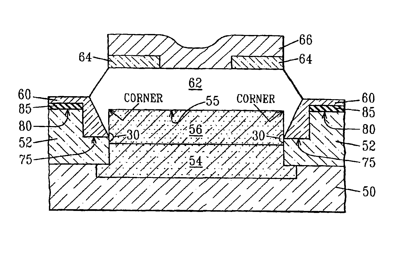
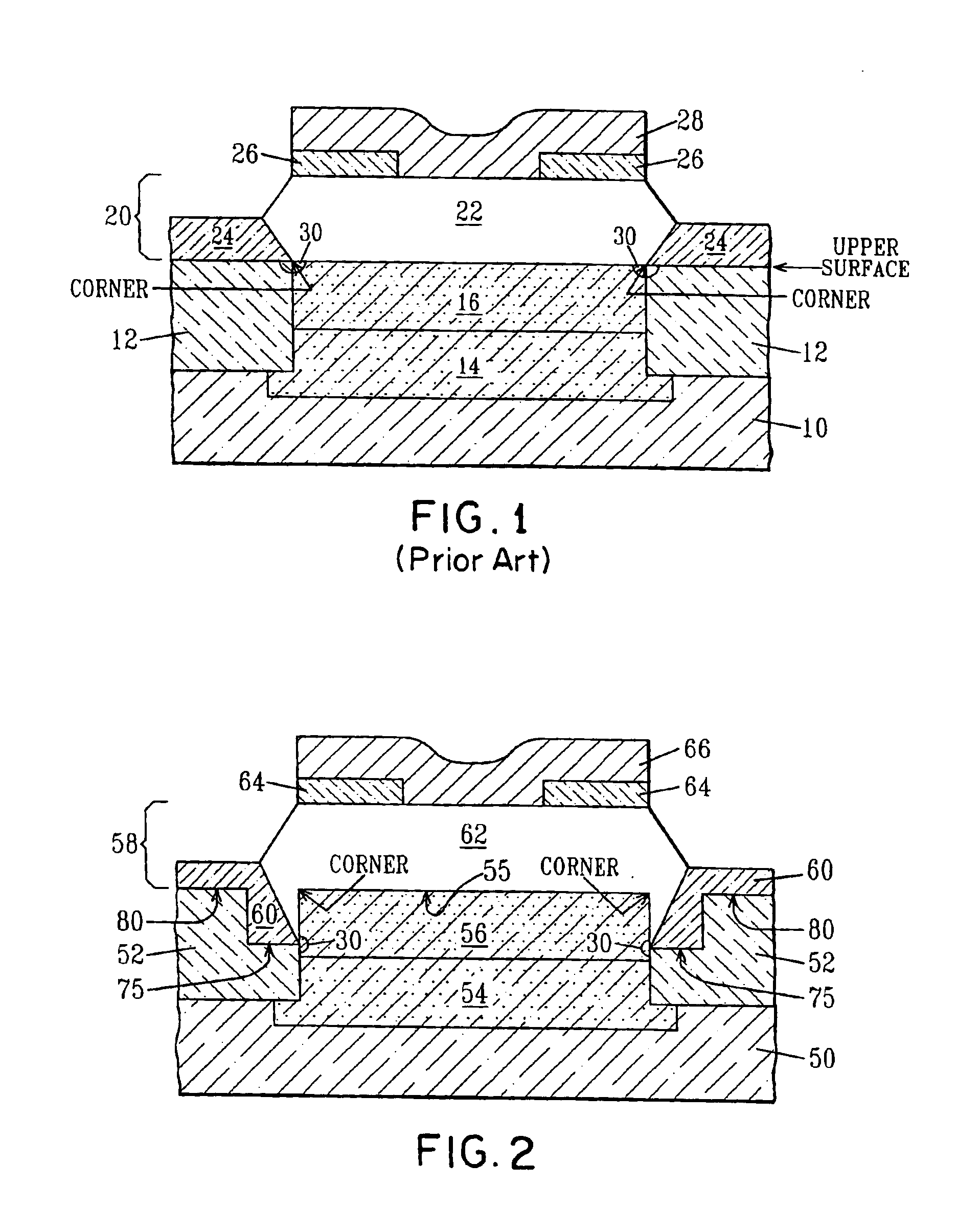
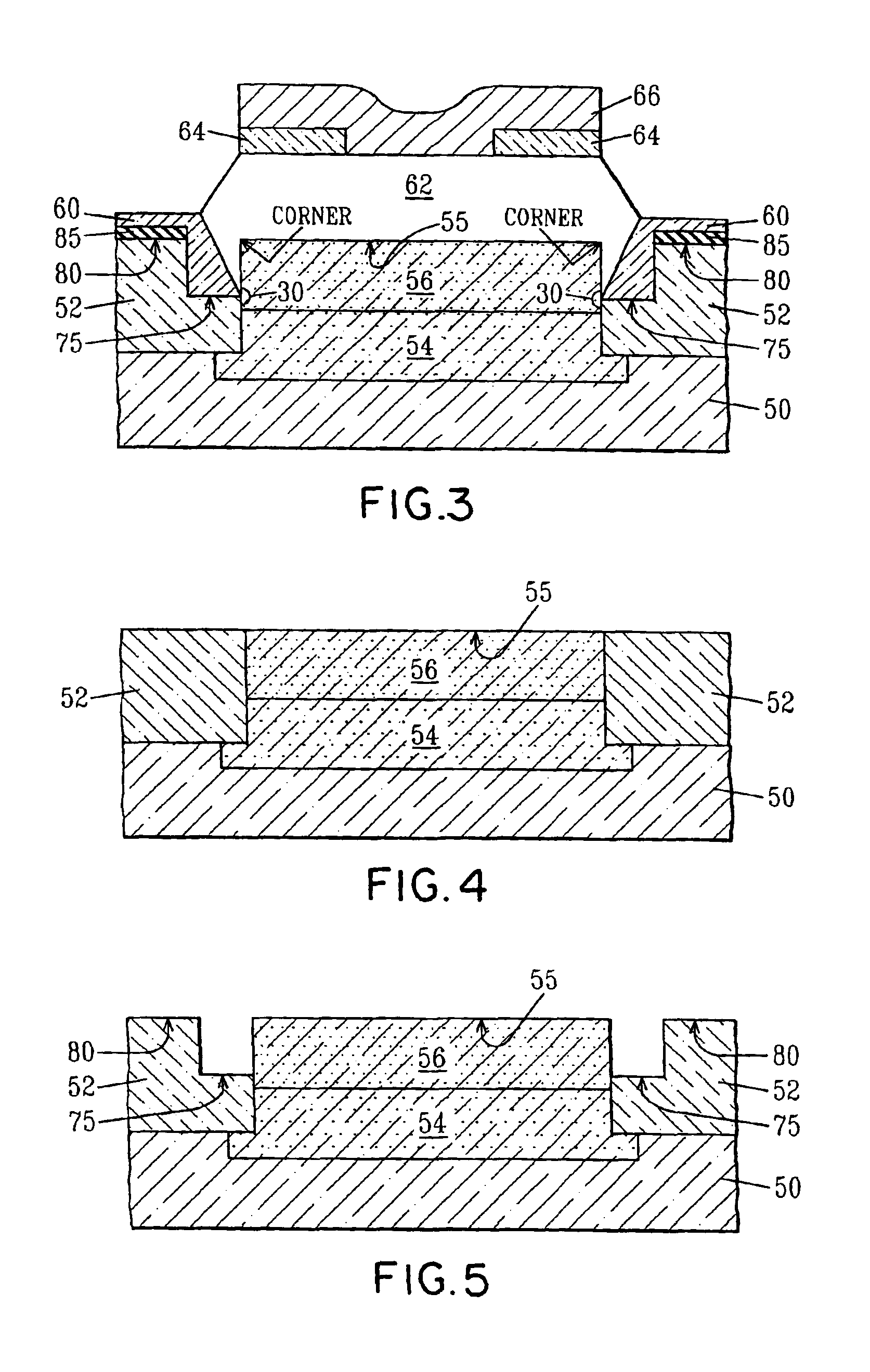
[0029]Reference is first made to FIG. 2 which represents a cross-sectional view of the inventive SiGe heterojunction bipolar transistor. Specifically, the SiGe heterojunction bipolar transistor comprises semiconductor substrate 50 of a first conductivity type (N or P) having sub-collector region 54 and collector region 56 formed therein. The substrate is further characterized as having an upper surface 55. Isolation regions 52 wh...


PUM


Abstract

A SiGe bipolar transistor including a semiconductor substrate having a collector and sub-collector region formed therein, wherein the collector and sub-collector are formed between isolation regions that are also present in the substrate is provided. Each isolation region includes a recessed surface and a non-recessed surface which are formed utilizing lithography and etching. A SiGe layer is formed on the substrate as well as the recessed non-recessed surfaces of each isolation region, the SiGe layer includes polycrystalline Si regions and a SiGe base region. A patterned insulator layer is formed on the SiGe base region; and an emitter is formed on the patterned insulator layer and in contact with the SiGe base region through an emitter window opening.

Description

RELATED APPLICATION[0001]This application is a divisional of U.S. application Ser. No. 09 / 769,640, filed Jan. 25, 2001 now U.S. Pat. No. 6,674,102.FIELD OF THE INVENTION[0002]The present invention relates to heterojunction bipolar transistors, and more particularly to a method of fabricating a SiGe heterojunction bipolar transistor wherein the base resistance is improved by employing an etching process that controls facet growth at the edges of the SiGe layer. Specifically, the present invention controls the facet growth by providing a recessed area in isolation regions that are present in the structure.BACKGROUND OF THE INVENTION[0003]Significant growth in both high-frequency wired and wireless markets has introduced new opportunities where compound semiconductors such as SiGe have unique advantages over bulk complementary metal oxide semiconductor (CMOS) technology. With the rapid advancement of epitaxial-layer pseudomorphic SiGe deposition processes, epitaxial-base SiGe heterojun...

Claims


Application Information

Patent Timeline
Patent Type & Authority Patents(United States)
IPC IPC(8): H01L21/331H01L21/02H01L29/737H01L29/66H01L21/20H01L29/73H01L29/732
CPCH01L29/66242H01L29/7378H01L29/73
Inventor COOLBAUGH, DOUGLAS DUANEDUPUIS, MARK D.GALLAGHER, MATTHEW D.GEISS, PETER J.PHILIPS, BRETT A.
Owner GLOBALFOUNDRIES INC
Why Eureka
Try Eureka