Copper interconnect structure having stuffed diffusion barrier

a diffusion barrier and copper interconnect technology, applied in the direction of semiconductor/solid-state device details, coatings, chemical vapor deposition coatings, etc., can solve the problems of cutting in the interconnection line, lack of excellent properties of cu, and inability to form a dense protective layer of cu

Inactive Publication Date: 2005-08-30
ASM INTERNATIONAL
View PDF44 Cites 77 Cited by
  • Summary
  • Abstract
  • Description
  • Claims
  • Application Information

AI Technical Summary

Problems solved by technology

Furthermore, the reduction in interconnection line width results in cutting in the interconnection line due to electromigration or stress migration.
However, Cu lacks excellent properties that Al has other than the low resistance and high melting point.
For example, Cu cannot form a dense protective layer such as Al2O3, has bad adhesive strength to SiO2 and is difficult to dry-etch.
Furthermore, copper's diffusion coefficient in SiO2 is known to be large, which decreases the ability of SiO2 to insulate between Cu lines.
As a result of copper's large diffusion coefficient in silicon and SiO2, the reliability of the semiconductor device is reduced.
However, when the diffusion barrier is deposited in a contact or trench structure using sputtering, step coverage deteriorates as the device size becomes smaller.
However, the development of new processes for forming a reliable diffusion barrier for Cu requires a considerably long period of time and this may delay commercialization of a semiconductor device employing a Cu interconnect structure.

Method used


Image

  • Copper interconnect structure having stuffed diffusion barrier
  • Copper interconnect structure having stuffed diffusion barrier
  • Copper interconnect structure having stuffed diffusion barrier

Examples


Embodiment Construction

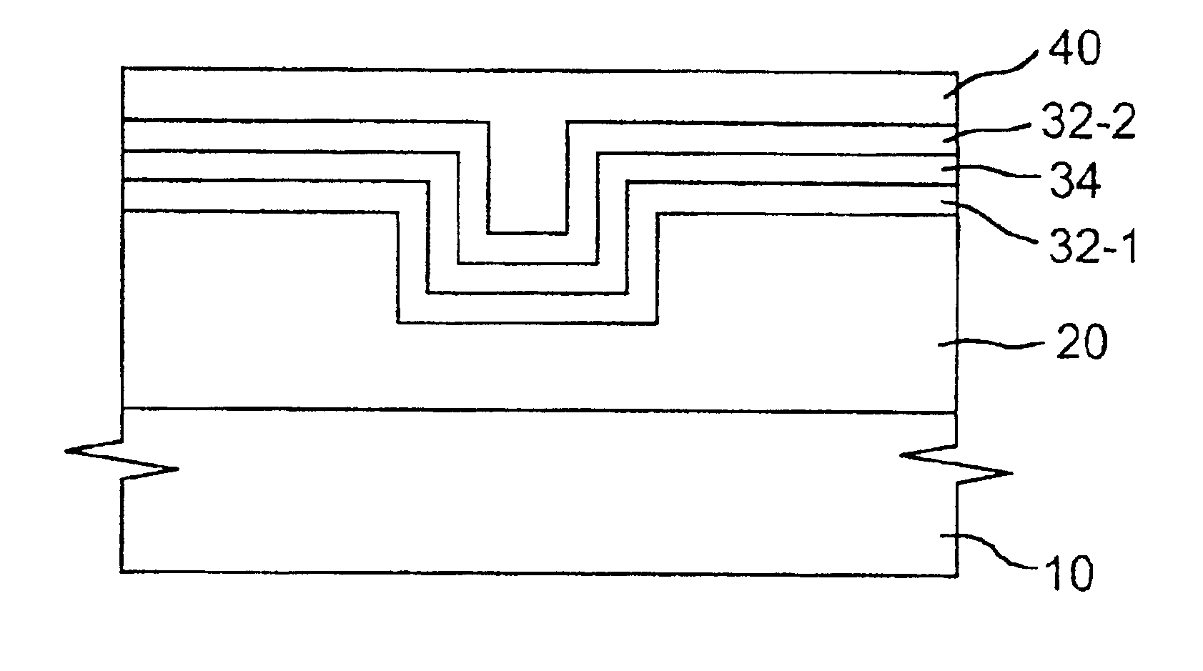
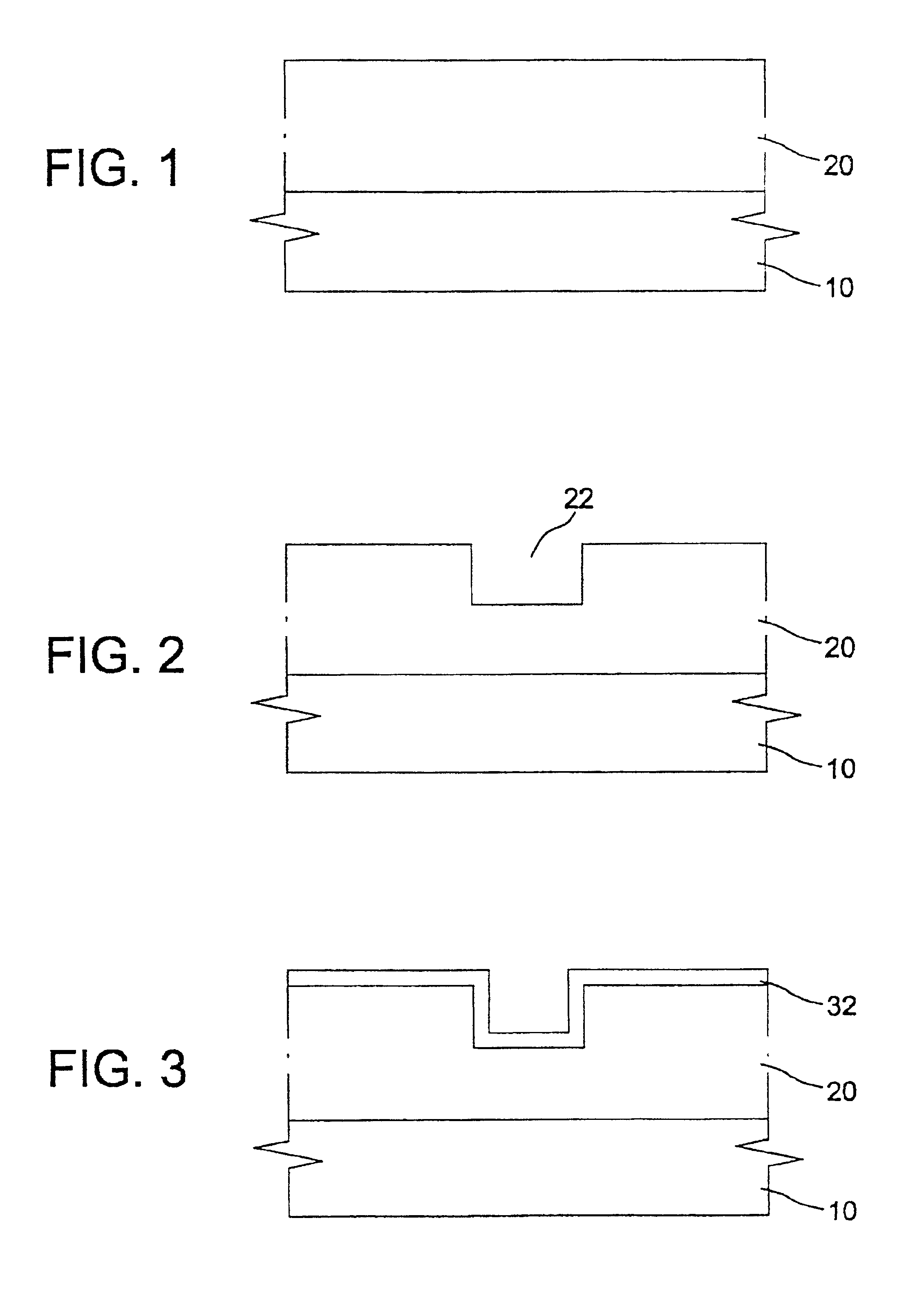
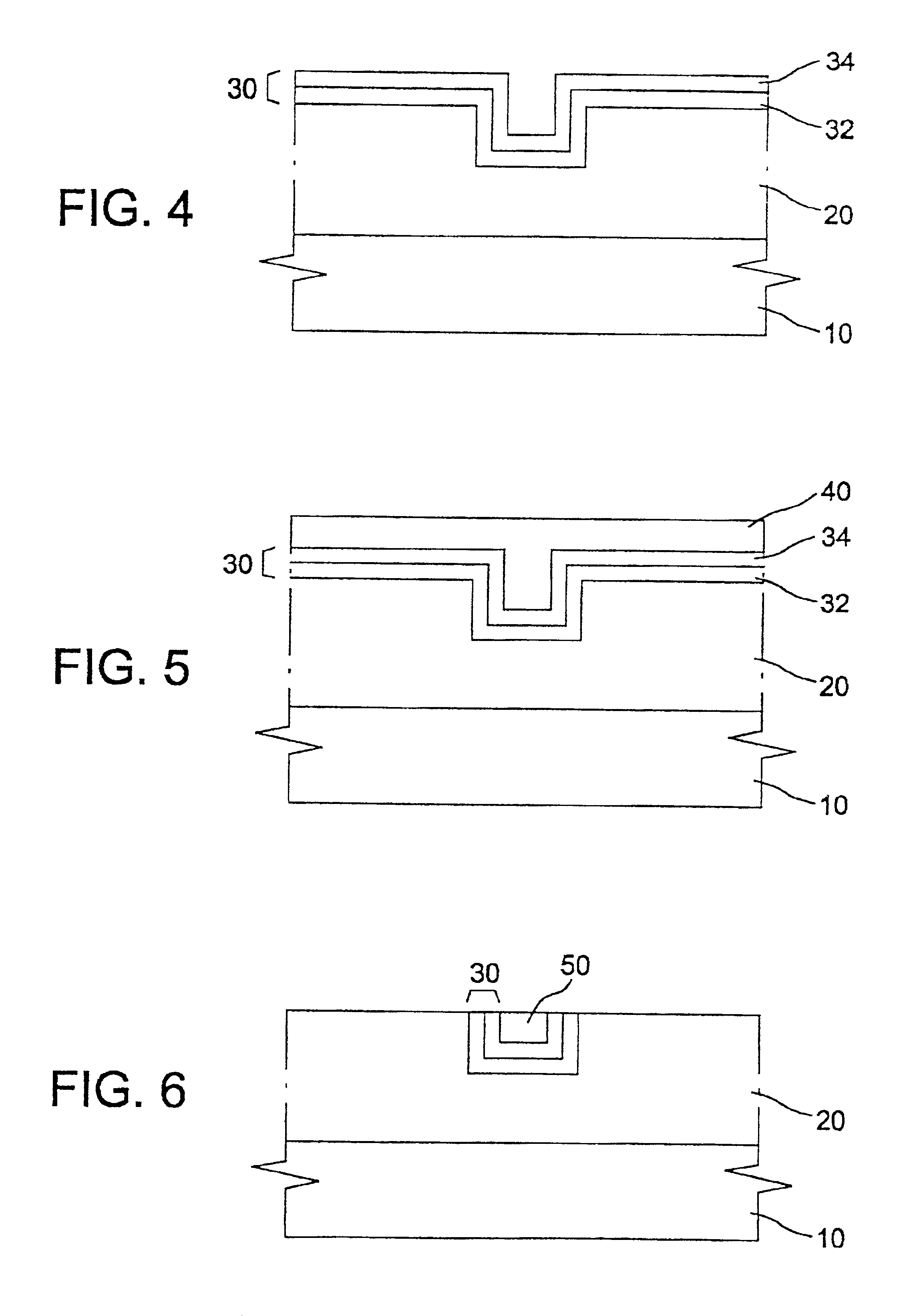
[0027]The present disclosure teaches processes for forming a diffusion barrier in the context of copper metallization, as well as diffusion barriers formed by these processes. However, the skilled artisan will appreciate that the present processes and structures have applications in other contexts.

[0028]The present invention will now be described in connection with preferred embodiments with reference to the accompanying drawings.

[0029]A diffusion barrier is a material that is inserted between two substances in order to prevent the substances from being mixing with each other due to diffusion. In a semiconductor device fabrication process, the diffusion barrier is used not only to prevent the diffusion between a substrate and interconnection material but also to block the interconnection material from diffusing into a dielectric film.

[0030]Diffusion barriers can be roughly classified into passive barriers, non-barriers, single crystal barriers, sacrificial barriers and stuffed barri...


PUM

PropertyMeasurementUnit
thickaaaaaaaaaa
thickaaaaaaaaaa
pressureaaaaaaaaaa

Abstract

The present invention provides a method of fabricating a semiconductor device, which could advance the commercialization of semiconductor devices with a copper interconnect. In a process of metal interconnect line fabrication, a TiN thin film combined with an Al intermediate layer is used as a diffusion barrier on trench or via walls. For the formation, Al is deposited on the TiN thin film followed by copper filling the trench. Al diffuses to TiN layer and reacts with oxygen or nitrogen, which will stuff grain boundaries efficiently, thereby blocking the diffusion of copper successfully.

Description

REFERENCE TO RELATED APPLICATIONS[0001]The present application claims priority under 35 U.S.C. §119 to Korean Patent Application Number 10-2000-0074025, filed Dec. 6, 2000.BACKGROUND OF THE INVENTION[0002]1. Field of the Invention[0003]The present invention generally relates to methods of fabricating a semiconductor device and, more particularly, to methods of forming interconnect structures in a semiconductor device fabrication process.[0004]2. Description of the Related Art[0005]A process of fabricating a semiconductor integrated circuit is roughly divided into the process of forming devices on a silicon substrate and the process of electrically connecting the devices. The latter is called an interconnection process or metallization, and is a key for improving yield rate and reliability in the fabrication of semiconductor devices as the devices become more highly integrated.[0006]A metal widely used as an interconnection material is aluminum (Al). However, as the integration of de...

Claims


Application Information

Patent Timeline
Patent Type & Authority Patents(United States)
IPC IPC(8): C23C16/34H01L21/28H01L21/285C23C16/20H01L21/3205H01L21/768H01L23/52H01L23/532
CPCH01L21/28562H01L21/76846H01L21/76855H01L21/76856H01L21/76858H01L23/53238H01L2924/0002H01L2924/00H01L21/28
Inventor KIM, KI-BUMSOININEN, PEKKA J.RAAIJMAKERS, IVO
Owner ASM INTERNATIONAL
Why Eureka
Try Eureka