Output buffer circuit with control circuit for modifying supply voltage and transistor size

a control circuit and supply voltage technology, applied in the field of impedance matching or interfacing technique, can solve the problem that the operation supply voltage of the individual semiconductor integrated circuit cannot be made impedance, and achieve the effect of reducing power consumption and speeding up data transmission

Inactive Publication Date: 2005-08-30
RENESAS ELECTRONICS CORP
View PDF4 Cites 11 Cited by
  • Summary
  • Abstract
  • Description
  • Claims
  • Application Information

AI Technical Summary

Benefits of technology

[0011][1] The invention intends to control both the power supply voltage and the transistor size of the external output buffer to thereby select the lowest supply voltage that achieves the impedance matching with the transmission line, and to thereby save the termination by a resistor, thus consequently achieving both the lowering of the power consumption and the speeding-up in the data transmission.

Problems solved by technology

For lowering the power consumption of the interface connecting the semiconductor integrated circuits, simply lowering the operational supply voltage to the individual semiconductor integrated circuit is impossible of making the impedance matching of the external output buffer of the individual semiconductor integrated circuit with the impedance of the transmission line, because the transistor characteristics are different each by the semiconductor integrated circuits.

Method used


Image

  • Output buffer circuit with control circuit for modifying supply voltage and transistor size
  • Output buffer circuit with control circuit for modifying supply voltage and transistor size
  • Output buffer circuit with control circuit for modifying supply voltage and transistor size

Examples


Embodiment Construction

[Master Integrated Circuit and Slave Integrated Circuit]

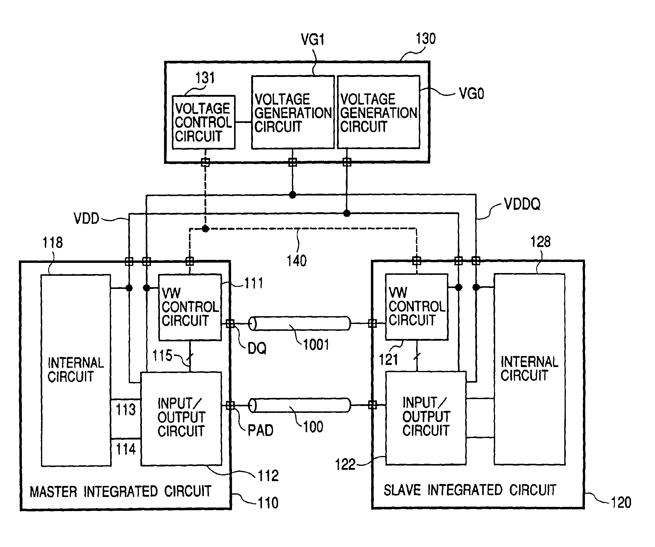
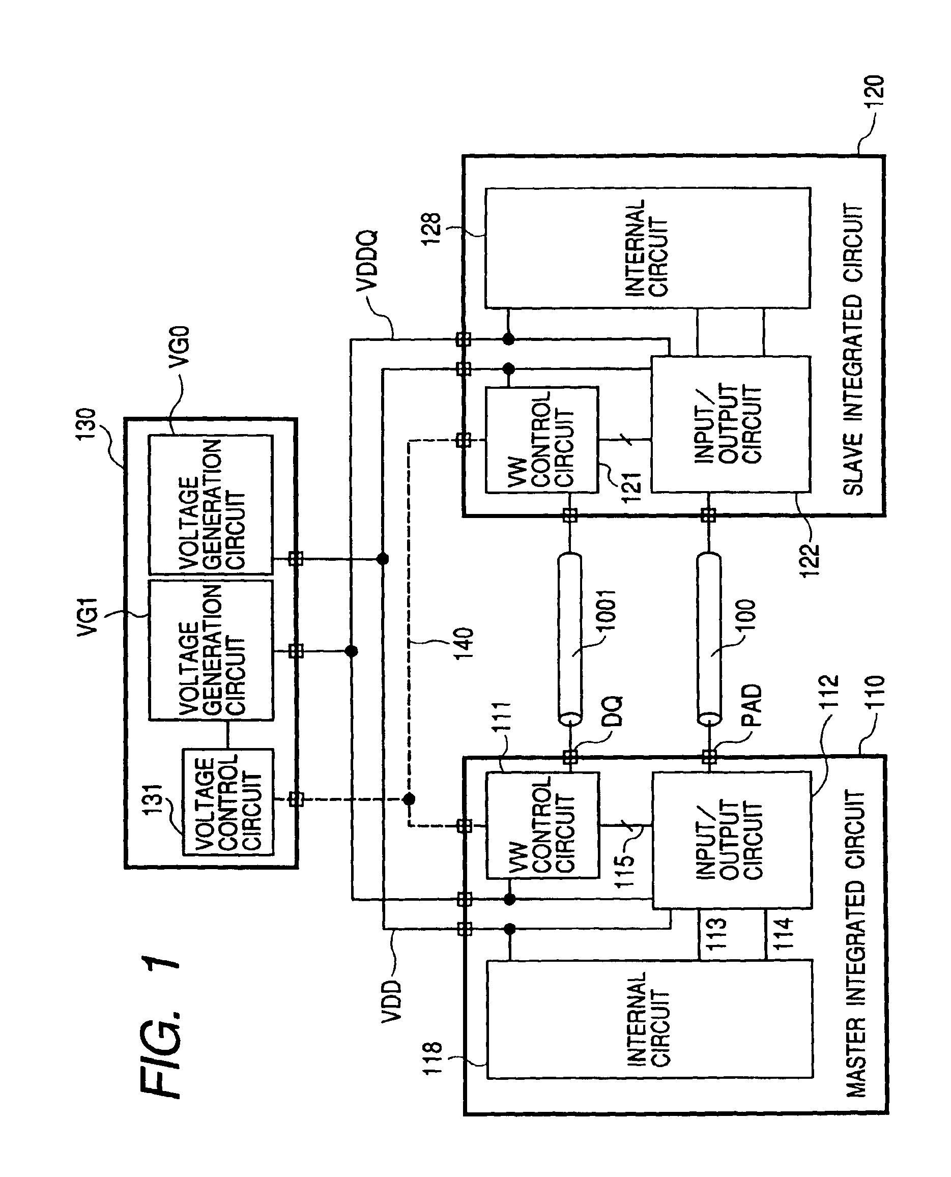
[0070]FIG. 1 illustrates an example of a data processing system that uses two units of integrated circuits relating to the present invention. The data processing system in the drawing performs data transmissions between a semiconductor integrated circuit 110 and a semiconductor integrated circuit 120 through a data line (transmission line) 100. Here, the example has only one data transmission line 100 for the data transmission, but the invention is applicable to the case having more transmission lines such as 8 lines.

[0071]The voltage generation circuit 130 supplies the semiconductor integrated circuits 110, 120 with common supply voltages. The voltage generation circuit VG0 supplies internal circuits 118, 128 of the semiconductor integrated circuits 110, 120 with a common operational supply voltage VDD, and the voltage generation circuit VG1 supplies input / output circuits (interface circuits) of the semiconductor integrated ci...


PUM


Abstract

In this invention, a control circuit (111) controls both the power supply voltage (VDDQ) and the transistor size of the external output buffer to thereby select the lowest supply voltage that achieves the impedance matching with the transmission line (100), to thereby save bus termination by a resistor, thus consequently achieving both the lowering of the power consumption and the speeding-up in the data transmission. The power consumption during the data transmission is proportional to the square of the supply voltage. If the operational supply voltage of the external output buffer is lowered, the power consumption will be reduced accordingly. If the operational supply voltage of the external output buffer is lowered, the impedance thereof will be increased apparently; and at the same time, if the transistor size of the external output buffer is increased, the increased impedance will be decreased. By bringing the output impedance (ON-resistance) of the external output buffer into conformity with the impedance of the transmission line, it becomes possible to output the signal without distortions on the waveform.

Description

[0001]This application is a Divisional application of nonprovisional U.S. Application No. 10 / 416,709 filed on May 14, 2003, which is a national stage application of PCT / JP00 / 08443 filed on Nov. 30, 2000. Priority is claimed based upon U.S. Application No. 10 / 416,709 filed on May 14, 2003, which claims the priority date of PCT / JP00 / 08443 filed on Nov. 30, 2000.TECHNICAL FIELD[0002]The present invention relates to an impedance matching technique or interfacing technique that satisfies the needs for lowering power consumption of semiconductor integrated circuits and speeding up data transmissions between the semiconductor integrated circuits. For example, the invention relates to a technique effective for use in the semiconductor integrated circuits such as microcomputers and memories, data processing systems that require an extremely lowered power consumption performance, such as mobile telephones and mobile information terminals, and data processing systems that require a fast data t...

Claims


Application Information

Patent Timeline
Patent Type & Authority Patents(United States)
IPC IPC(8): H04L25/02G06F1/32H03K19/00H03K19/003
CPCG06F1/3228G06F1/324G06F1/3296H03K19/0005H03K19/0016H04L25/0278H04L25/03885H04L25/028H04L25/0292Y02B60/1217Y02B60/1285Y02D10/00
Inventor SATOU, TAKASHIMATSUI, SHIGEZUMILEE, PETERYOKOMIZO, GOUICHI
Owner RENESAS ELECTRONICS CORP
Why Eureka
Try Eureka