Programming flash memory via a boundary scan register

a programming flash memory and boundary scan technology, applied in the field of boundary scan register programming flash memory, can solve the problems of inability to simultaneously program a number of integrated semiconductor components mounted on the same circuit board, insufficiently achieving the practical success of this standard, and inability to achieve the effect of reducing the programming effor

Active Publication Date: 2005-08-30
NOKIA SIEMENS NETWORKS GMBH & CO KG +1
View PDF5 Cites 47 Cited by
  • Summary
  • Abstract
  • Description
  • Claims
  • Application Information

AI Technical Summary

Benefits of technology

[0020]To reduce the programming effort, in accordance with the invention, the data of the circuit diagram or of the network list derived from it, which defines the configuration of the interface between the flash memory to be programmed and the ASIC, is stored in a further file (BSDL file) so that the flash memory to be programmed, after adaptation of the features of the flash memory to IEEE Standard 1532 can be programmed via a JTAG interface in the same way as a programmable logic device (PLD).

Problems solved by technology

Nor is there a uniform definition of test vector formats for data interchange contained in IEEE-Standard 1149.1.
Even if the previously described theory of IEEE Standards 1532 appears to promise much, it is in no way sufficient for the practical success of this Standard.
However using this method produces a number of problems: Thus for example for programming a flash memory creation of a program is relatively expensive since the configuration (i.e. the connections between ASIC and Flash memory) is taken from the circuit diagram or from the network list derived from it and the BSDL file of the ASIC must be included.
Furthermore simultaneous programming of a number of integrated semiconductor components mounted on the same circuit board is not currently possible.
Above and beyond this, with conventional methods burst mode is also not possible since with each write cycle the programming data has to be shifted into the ASIC as well as the addresses and the control bits too as a rule.

Method used


Image

  • Programming flash memory via a boundary scan register
  • Programming flash memory via a boundary scan register
  • Programming flash memory via a boundary scan register

Examples


Embodiment Construction

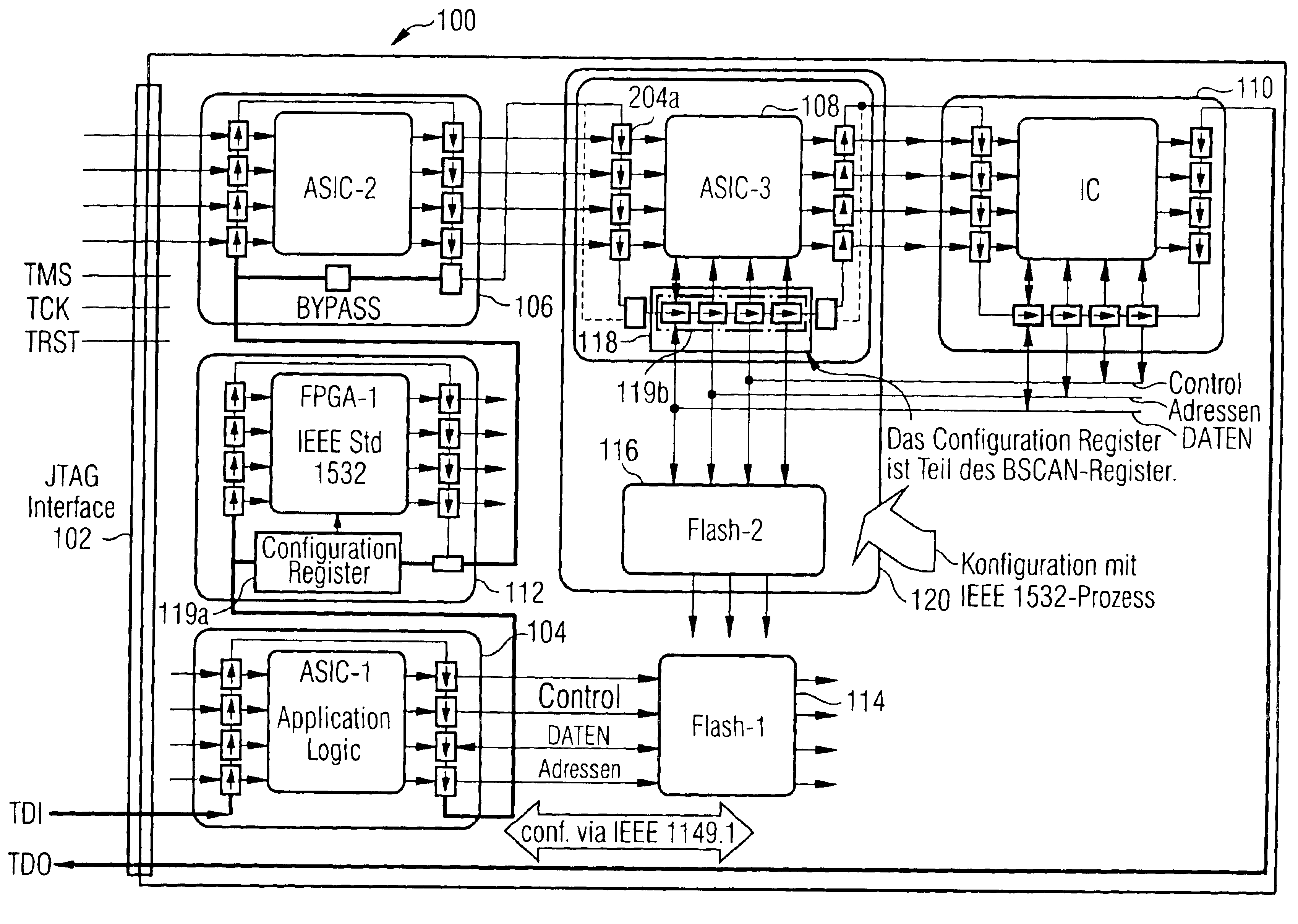
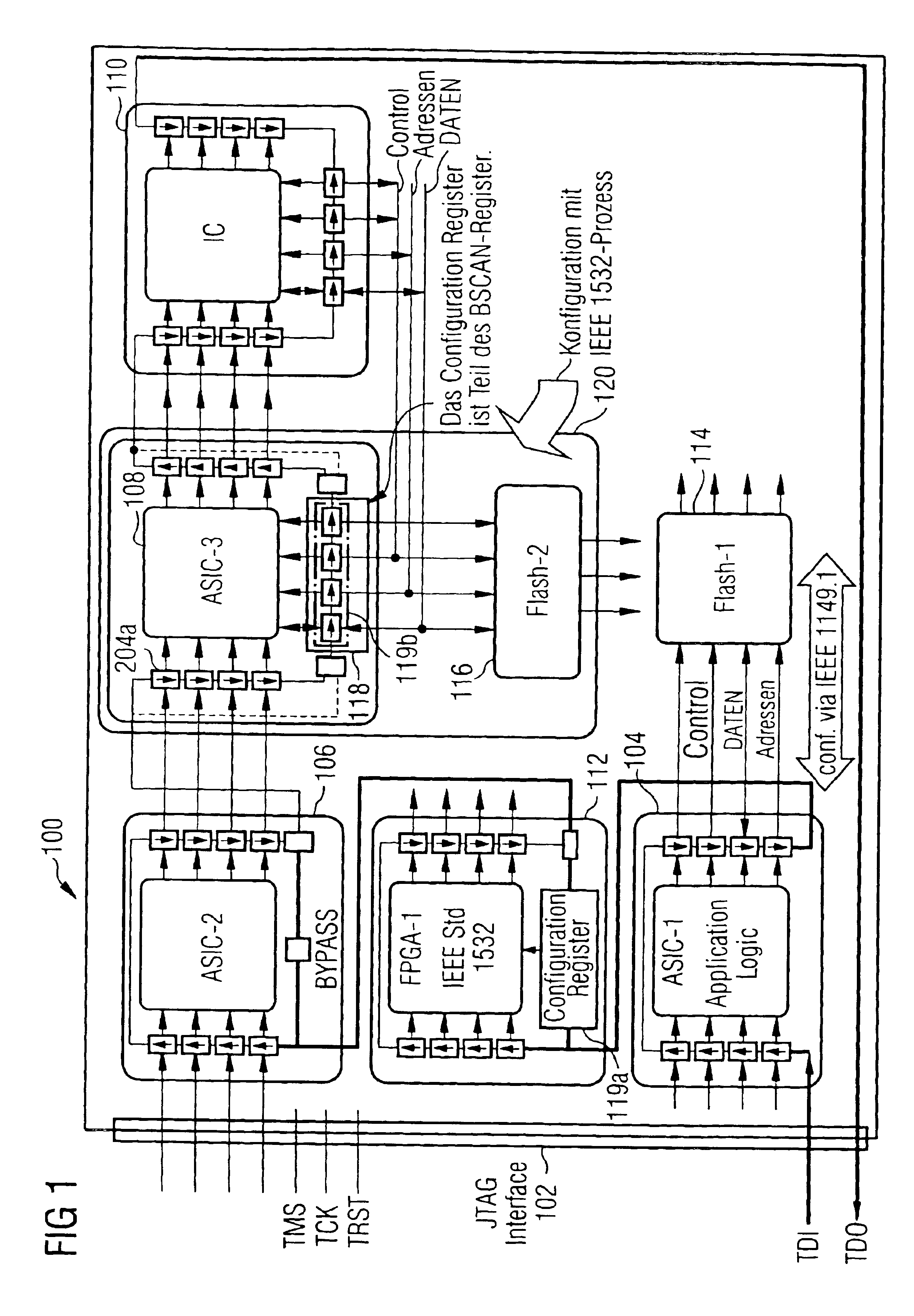
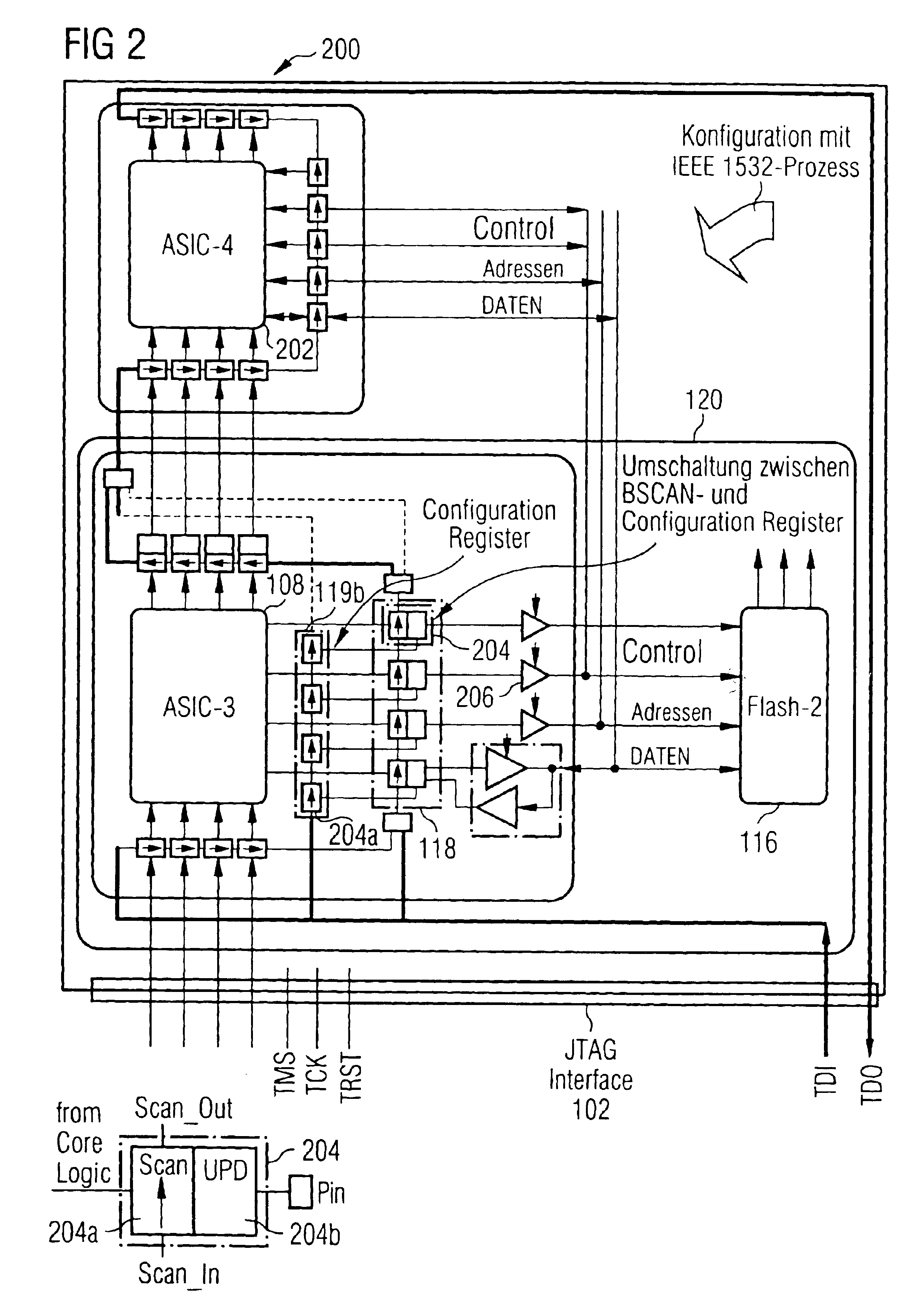
[0025]The invention is explained in more detail below using the exemplary embodiments illustrated in FIGS. 1 to 3. The meaning of the symbols provided with reference numbers in FIGS. 1 to 3 can be taken from the enclosed list of reference numbers.

[0026]Within the context of an exemplary embodiment of the present invention there is provision for an ASIC 108, suitably adapted for on-board programming and In-System Configuration (ISC) of a flash memory 116, which can be controlled via a JTAG interface 102 in accordance with IEEE Standard 1149.1 and reprograms or configures the flash memory 116 even during operation. In accordance with the invention, ASIC 108 and flash memory to be programmed 116 are considered with the context of IEEE Standard 1532 as contiguous unit 120 (see FIGS. 1 and 2). As a result it makes no difference whether flash memory 116 is inside or outside ASIC 108.

[0027]If one gives this ASIC 108 characteristics in accordance with IEEE Standard 1532, the flash memory 11...


PUM


Abstract

A method and parallel interface for on-board programming and / or In-System Configuration of a flash memory mounted on a printed circuit board by controlling its inputs with the aid of an ASIC mounted on the same circuit board via a Boundary Scan register of which the output signals are provided for activating or deactivating a write operation. The architecture description of the ASIC, flash memory, and the data format of the program and configuration data are stored in a Boundary-Scan Description Language file. The circuit board can be controlled via a JTAG interface suitable for performing function testing of the flash memory for input or output of standard bus signals and for input of the control signals of the ASIC. To reduce the programming effort, the data of the circuit diagram or of the network list derived from it is stored in the BSDL file.

Description

CLAIM FOR PRIORITY[0001]This application claims priority to German Application No. 10244757.8, filed Sep. 25, 2002, the contents of which are hereby incorporated by reference.TECHNICAL FIELD OF THE INVENTION[0002]The underlying invention is based on a method and an interface for on-board programming and / or In-System Configuration (ISC) of flash memory mounted on a printed circuit board by controlling its inputs with the aid of an application-specific integrated circuit mounted on the same circuit board via a Boundary Scan (BSCAN) register of which the outputs are provided for activating or deactivating a write operation.BACKGROUND OF THE INVENTION[0003]The Boundary Scan technique (BSCAN) is a standardized method for board tests, that was formally approved in 1990 as industry standard IEEE 1149.1 for Test Access Port (TAP) and Boundary Scan (BSCAN) architectures. Connection tests at board level in the production of complex printed circuit boards (PCBs) are based on this specification...

Claims


Application Information

Patent Timeline
Patent Type & Authority Patents(United States)
IPC IPC(8): G11C16/10G11C5/06G11C16/04G11C16/06G11C29/00
CPCG11C16/102G11C16/04G11C2029/3202
Inventor KRAUSE, KARLHEINZTIEMEYER, ELKE
Owner NOKIA SIEMENS NETWORKS GMBH & CO KG
Why Eureka
Try Eureka