Semiconductor device

a technology of integrated circuits and semiconductors, applied in semiconductor devices, digital storage, instruments, etc., can solve the problems of increasing power consumption, reducing breakdown voltage, increasing the number of elements, etc., and achieve the effect of ensuring stable operation of semiconductor devices

Inactive Publication Date: 2005-08-30
RENESAS ELECTRONICS CORP
View PDF7 Cites 17 Cited by
  • Summary
  • Abstract
  • Description
  • Claims
  • Application Information

AI Technical Summary

Benefits of technology

[0010]Therefore, an object of the present invention is provide means for supplying an internal power-supply voltage stably and flexibly to solve the problem of operating voltage supply caused by a drop of the power-supply voltage supplied from the outside.
[0013]Preferably, the third operating voltage is generated as follows. The first operating voltage is increased to a fourth operating voltage higher than the first operating voltage by a voltage up-converter. Then, the fourth operating voltage is dropped to the third operating voltage by a voltage down-converter. Hence, the operation of the semiconductor device can be kept stable even in the case where a power supply with a relatively fluctuating voltage as the first operating voltage is used.

Problems solved by technology

Problems against a flow of this technique are increase of power consumption owing to increase of the number of elements and reduction of breakdown voltage owing to the miniaturization of the circuit elements.
In order to mix DRAMs in the aforementioned situation, how to supply electric power to the DRAM circuit block is a problem to be solved.
The first power supply VDDQ, however, has a problem that power-supply noise is large because VDDQ is used for I / O circuits in which a relatively large current flows.
That is, when the first power supply VDDQ is used directly for DRAM circuits, there is a fear that VDDQ cannot fulfil its performance sufficiently.
On the other hand, it is also to be feared that the voltage of the second power supply VDD may be too low to supply power to the DRAM circuit block in the future because reduction of the voltage is progressing radically.
That is, though a word line drive voltage needs the highest voltage in the DRAM circuit block, it is supposed that difficulty occurs in an aspect of power efficiency etc. when a technique which uses a charge pump voltage up-converter for generating the word line drive voltage from VDD is used.
It is supposed that, the aforementioned problem occurs not only in the DRAM circuit block but also in analog circuits such as an AD converter, a DA converter and a PLL; circuits such as a flash memory; or logic circuits such as a microprocessor and a DSP which operate with a super-low voltage of 0.7 V or lower and which are sensitive to the fluctuation of the power-supply voltage.

Method used


Image

  • Semiconductor device
  • Semiconductor device
  • Semiconductor device

Examples


embodiment 1

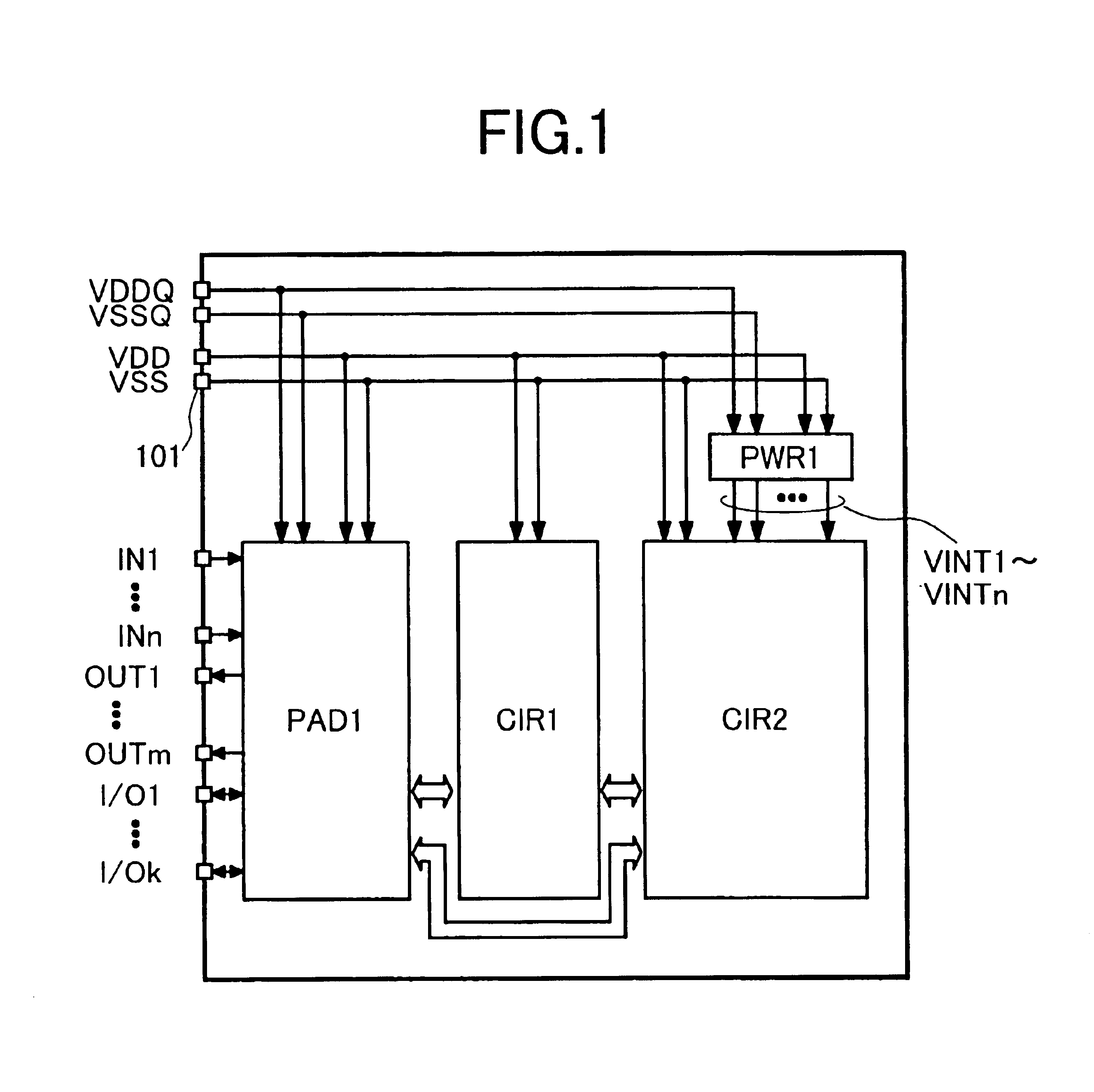
[0052]FIG. 1 shows the overall configuration of an embodiment of a semiconductor integrated circuit chip (hereinafter simply referred to as “silicon chip” or “chip”) according to the present invention. The chip is supplied with I / O power-supply voltages VDDQ and VSSQ and core power-supply voltages VDD and VSS from the outside of the chip through individual power supply pads 101 respectively. VDDQ is a power supply for the I / O pins. VSSQ is the ground for the I / O pins. VDD is a core power supply voltage for the core circuitry. VSS is the ground for the core circuitry. Generally, an I / O voltage (VDDQ−VSSQ) is higher than a core voltage (VDD−VSS). A specific combination of power-supply voltages is not specifically limited. For example, a combination of an I / O voltage of about 3.3 V with a core voltage of about 1.5 V may be used typically. Generally, because both VSSQ and VSS have the same ground potential (GND) ideally, the I / O power-supply voltage and the core power-supply voltage wil...

embodiment 2

[0089]In Embodiment 2, a modified example of the overall configuration of the semiconductor integrated circuit as a subject of the present invention shown in FIG. 1 as Embodiment 1 will be described.

[0090]In comparison with FIG. 1, FIG. 19 shows an example in which the reference potential VSSQ for the I / O power supply and the reference potential VSS for the core power supply are shared with each other as common VSS so that the common VSS is received from a common power-supply pad and in which the reference potential power-supply wiring patterns in the inside are also shared with each other. When, for example, electric power consumed by the I / O circuit is so low that the peak current is small, it is unnecessary to separate the I / O power supply from the core power supply. In this case, the number of pins of the chip as a whole can be reduced when VSS is shared with VSSQ.

[0091]FIG. 20 shows an embodiment in the case where the pad and the power supply for VDDQ and VSSQ which are used in...

embodiment 3

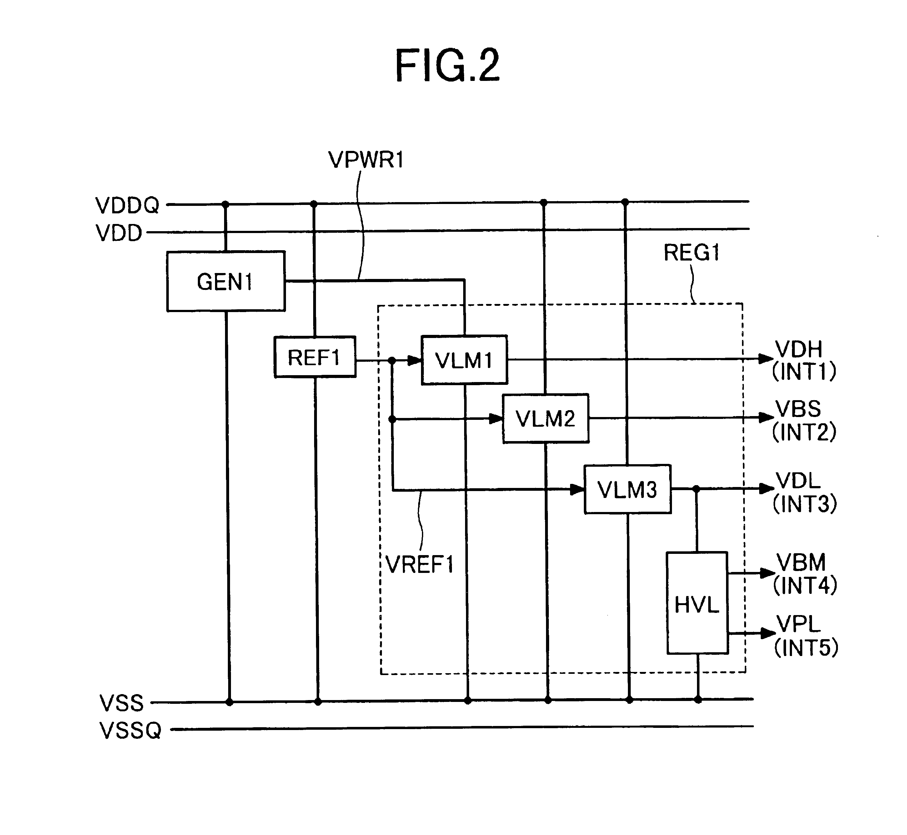
[0104]A specific example and a modified example of arrangement on a chip in the overall configuration of the semiconductor integrated circuit as a subject of the present invention described in Embodiments 1 and 2 will be described below as Embodiment 3. If GEN1, REF1 and REG1 are arranged in the following portions in a chip, various effects can be obtained.

[0105]FIG. 24 shows a physical layout image of a chip according to the present invention. PAD1 is a region in which pads for signal interface to the outside are arranged. The location of PAD1 is not specifically limited but, in this embodiment, PAD1 is located in the periphery of the chip. One GEN1 and one REF1 are formed on the chip and located in the left upper portion of the chip. This embodiment illustrates the case where the second internal circuit CIR2 is further divided into two parts, CIR2a and CIR2b. Typically, that which is equivalent to this case is the case where CIR2 provided as a DRAM circuit is divided into a plural...


PUM


Abstract

A semiconductor device having a first circuit block supplied with a first operating voltage, a second circuit block supplied with a second operating voltage, a voltage generating circuit for generating a third operating voltage in response to the first operating voltage, and a third circuit block supplied with the third operating voltage. Preferably, the third operating voltage is generated such that the first operating voltage is increased to a fourth operating voltage by a voltage-up converter, and then the fourth operating voltage is dropped to the third operating voltage by a voltage down-converter. Hence, a power supply operating internally stably in spite of use of a relatively fluctuating voltage can be provided even in the case where a power-supply voltage is dropped.

Description

[0001]This is a continuation application of U.S. Ser. No. 10 / 319,511, filed Dec. 16, 2002 now U.S. Pat. No. 6,711,071, which is a continuation application of U.S. Ser. No. 10 / 067,902, filed Feb. 8, 2002, now U.S. Pat. No. 6,515,918, which is a continuation application of U.S. Ser. No. 09 / 639,742, filed on Aug. 15, 2000, now U.S. Pat. No. 6,366,506.BACKGROUND OF THE INVENTION[0002]The present invention relates to a semiconductor integrated circuit device and particularly to a high-speed low-power semiconductor integrated circuit device having various forms of circuit blocks mounted thereon by mixture.[0003]A list of references in this specification is as follows. The references will be referenced by reference numerals.[Reference 1]: M. Tsukude et al., 1997 IEEE International Solid-State Circuits Conference (ISSCC) Digest of Technical Papers, February 1997, pp.66-67[Reference 2]: JP-A-8-234851 laid open on Sep. 13, 1966[Reference 3]: S. Fujii et al., 1986 IEEE International Solid-Stat...

Claims


Application Information

Patent Timeline
Patent Type & Authority Patents(United States)
IPC IPC(8): G11C5/14G11C11/413G05F1/56G11C11/407H01L21/822H01L27/04
CPCG11C5/14G11C5/147G11C11/407
Inventor MIZUNO, HIROYUKIWATANABE, TAKAOHIRAKI, MITSURUTANAKA, HITOSHI
Owner RENESAS ELECTRONICS CORP
Why Eureka
Try Eureka