Selective dry etching of tantalum and tantalum nitride

a dry etching and tantalum technology, applied in the field of dry etching process, can solve the problems of rc time delay, selective removal of tasub>x/sub>n/sub>layer, and difficult process of selective removal of tasub>y/sub>layer, and achieve the effect of reducing the rc time delay

Inactive Publication Date: 2005-09-06
TEXAS INSTR INC
View PDF5 Cites 19 Cited by
  • Summary
  • Abstract
  • Description
  • Claims
  • Application Information

AI Technical Summary

Benefits of technology

[0004]Tantalum and tantalum nitride layers are often formed during integrated circuit formation. The instant invention recites a method to selectively etch tantalum nitride. The instant invention comprises exposing a semiconductor substrate comprising at least one tantalum layer and/or tantalum nitride layer...

Problems solved by technology

One of the primary challenges in integrated circuit fabrication is reducing the RC time delay.
Using existing methods the selective removal of the TaxNy layer is a very difficult process.
CMP processes are often used to remove the exposed TaxNy layer 30 but this often results in dishing...

Method used


Image

  • Selective dry etching of tantalum and tantalum nitride
  • Selective dry etching of tantalum and tantalum nitride

Examples


Embodiment Construction

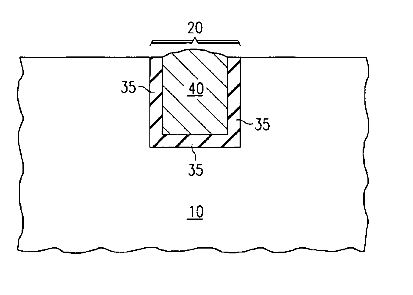
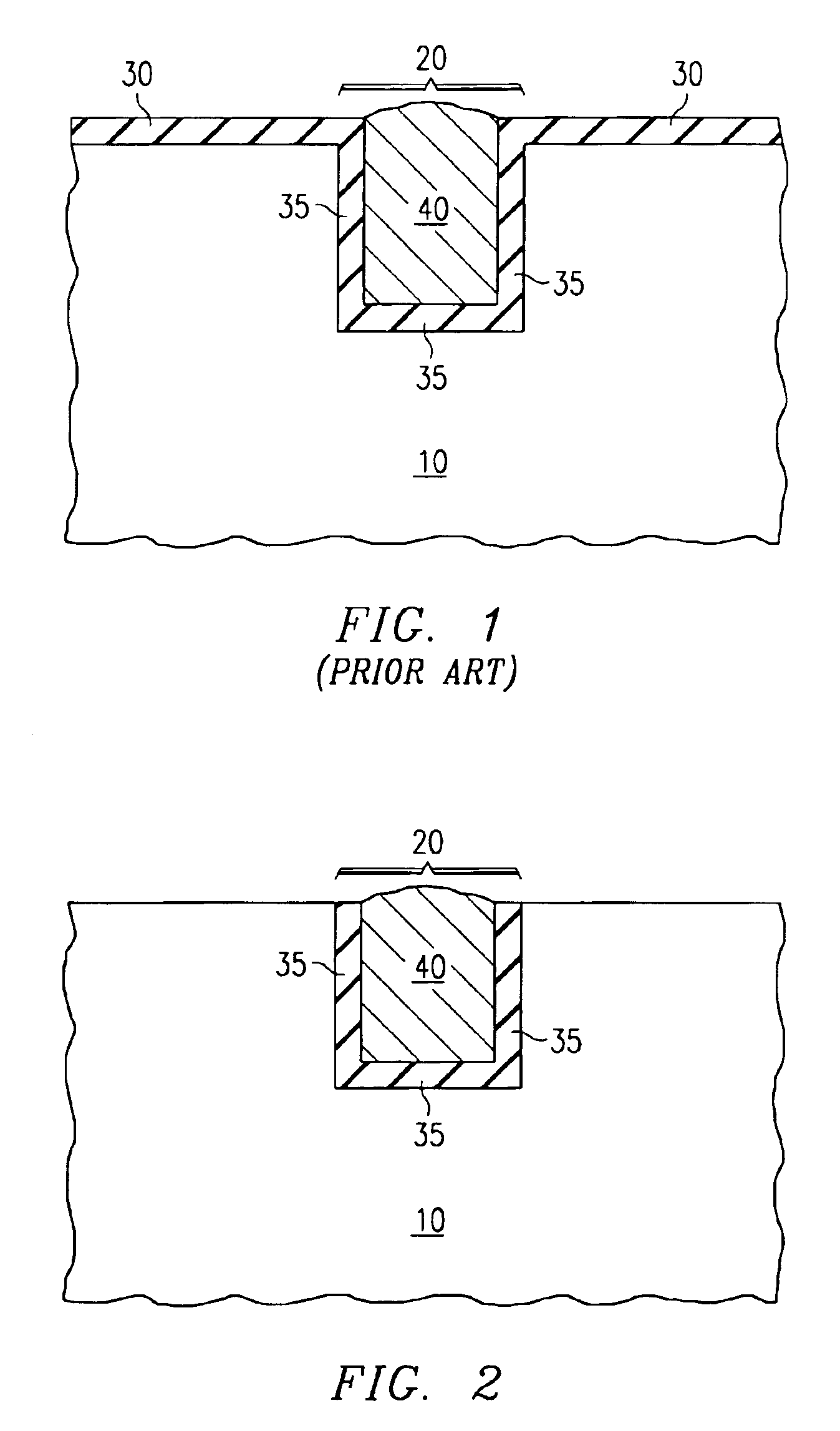
[0008]A two step dry etch process is used to selectively etch TaxNy and / or Tantalum (Ta). The subscripts x and y in the chemical symbol for tantalum nitride (i.e. TaxNy) represent integer numbers that depend on the form of the tantalum nitride alloy. The etch process of the instant invention will selectively etch all forms of tantalum nitride alloys and well as tantalum metal. The process conditions are described in the following table:

[0009]

ReducingOxidizingIndicesUnitsStep 1Step 2WaferCelsius>60TemperaturePressuremilliTorr500-900500-900N2Sccm 250-10000NH3Sccm1000-40000O2Sccm01000-5000H2Sccm00C2F4Sccm0 20-100PowerWatts 700-1200 800-1800

[0010]As shown in above table, the first step of the process comprises a plasma process with nitrogen (N2) and ammonium (NH3) as the active gases. In addition to N2 and NH3 other gases, including carrier gases such as argon, can be present in the chamber without departing from the instant invention. In an embodiment of the instant invention the flow ...


PUM

PropertyMeasurementUnit
Angleaaaaaaaaaa
Angleaaaaaaaaaa
Plasma poweraaaaaaaaaa

Abstract

The invention describes a method for the selective dry etching of tantalum and tantalum nitride films. Tantalum nitride layers (30) are often used in semiconductor manufacturing. The semiconductor substrate is exposed to a reducing plasma chemistry which passivates any exposed copper (40). The tantalum nitride films are selectively removed using an oxidizing plasma chemistry.

Description

FIELD OF THE INVENTION[0001]The present invention relates to a dry etching process for the selective removal of tantalum and tantalum nitride layers. The dry etch process used etches tantalum and tantalum nitride without significantly attacking copper layers and silicon oxide based dielectric layers.BACKGROUND OF THE INVENTION[0002]The use of copper for forming the metal interconnect lines in integrated circuits is finding increasing usage due to the superior properties of copper compared to the widely used aluminum lines. One of the primary challenges in integrated circuit fabrication is reducing the RC time delay. An important component of the RC time delay is the resistance and the capacitance present in the metal lines that connect the various devices that comprise the integrated circuit. The resistivity of copper is 1.72×10⁻⁶ Ohm-cm versus that of aluminum which is 2.82×10⁻⁶ Ohm-cm. This reduced resistivity will reduce the RC delay associated with copper lines. In addition copp...

Claims


Application Information

Patent Timeline
IPC IPC(8): C23F4/00H01L21/02H01L21/321H01L21/3213H01L21/3065H01L21/44H01L21/768
CPCC23F4/00H01L21/32115H01L21/32136H01L21/76838H01L21/7684H01L21/76843H01L21/76862H01L21/76865
Inventor EISSA, MONA M.YOCUM, TROY A.
Owner TEXAS INSTR INC
Why Eureka
Try Eureka