Small grain size, conformal aluminum interconnects and method for their formation

a technology of aluminum interconnects and conformal aluminum, applied in the direction of semiconductor devices, semiconductor/solid-state device details, electrical apparatus, etc., can solve the problems of difficult to obtain adequate step coverage, non-conformal layers, and unsatisfactory interconnects, so as to improve the ohmic characteristics of the contact, diffuse easily through the interconnect structure, and reduce the resistance contact

Inactive Publication Date: 2005-09-20
MICRON TECH INC
View PDF22 Cites 10 Cited by
  • Summary
  • Abstract
  • Description
  • Claims
  • Application Information

AI Technical Summary

Benefits of technology

[0010]In particular, according to another aspect of the method of the present invention, a titanium silicide layer is formed between the first titanium nitride layer and the underlying active device region to further improve the ohmic characteristics of the contact. Titanium silicide has an intermediate crystallographic structure between that of silicon in the active device region and titanium nitride. Thus, electronic carriers are able to diffuse easily through the interconnect structure.
[0011]The crystal structure and grain size of the underlayers are controlled to promote subsequent formation of a small grain size, conformal aluminum film in an interconnect. The aluminum film formed according to the method of the invention has a polycrystalline orientation, with grain sizes of less than approximately 0.25 microns. Thus, interconnects are formed with aluminum instead of tungsten, providing a lower resistivity contact to adjacent active device regions. Furthermore, such aluminum films are more conformal due to their smaller grain sizes. Vias are thus able to be filled with such aluminum to provide an interconnect structure substantially free of unwanted voids.

Problems solved by technology

However, interconnects are not ideal and typically exhibit near linear characteristics at best.
One significant concern in depositing metal into a via is obtaining adequate step coverage of the via, particularly obtaining adequate step coverage is difficult when the vias have high aspect ratios (i.e. a large ratio of height to width of the via), as seen more often as IC densities increase.
However, to date, CVD aluminum exhibits rough, nonconformal layers on complex topographies, prior to surface modification.
This is undesirable because voids often develop within a via, due to the roughness of the CVD aluminum.
Such voids severely increase the resistivity of a contact and degrade device performance by not providing uniform connection across an interconnect.

Method used


Image

  • Small grain size, conformal aluminum interconnects and method for their formation
  • Small grain size, conformal aluminum interconnects and method for their formation
  • Small grain size, conformal aluminum interconnects and method for their formation

Examples


Embodiment Construction

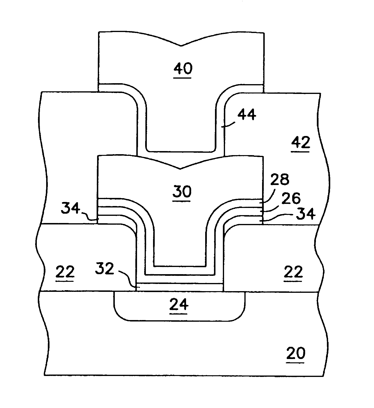
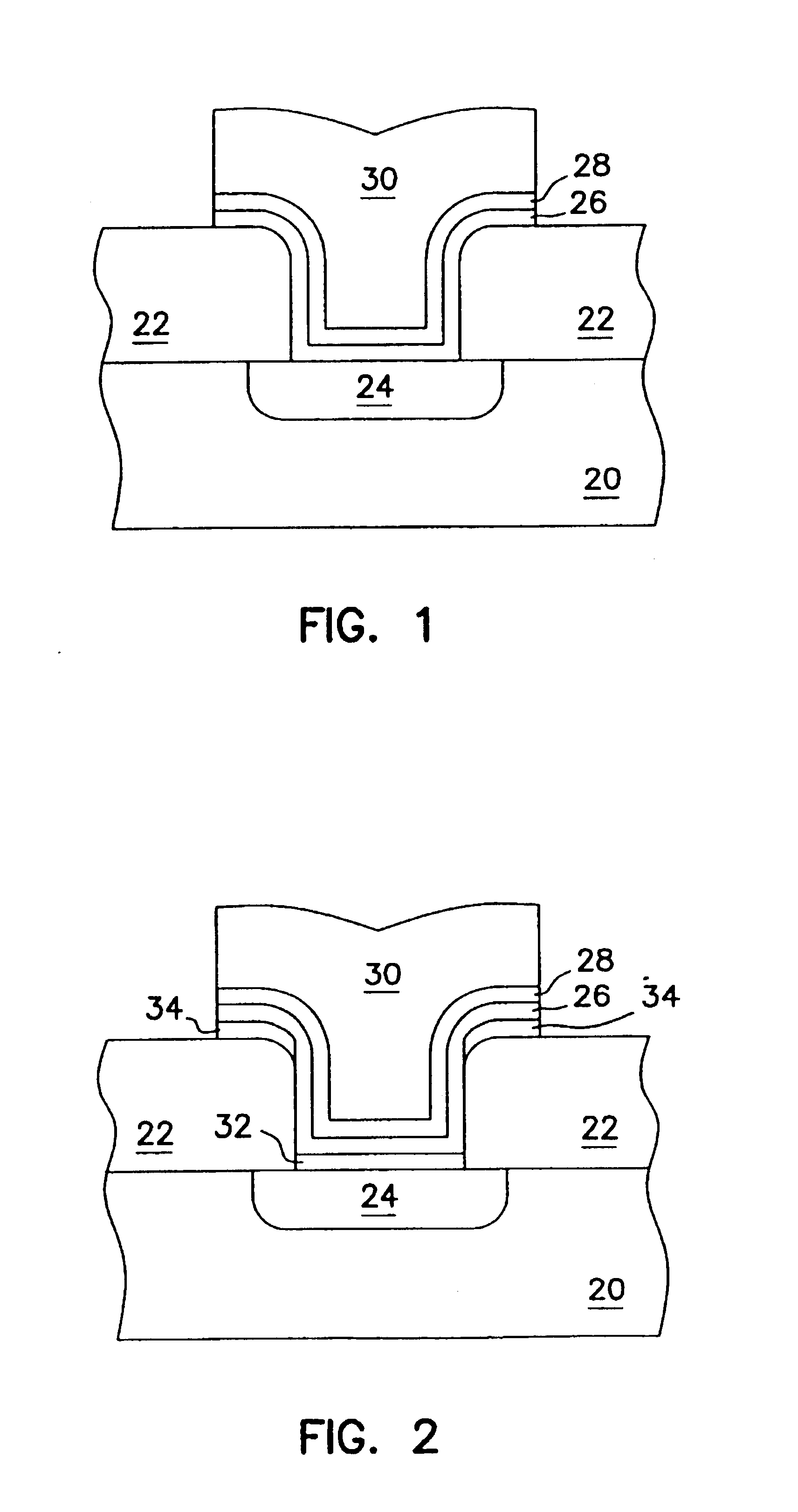
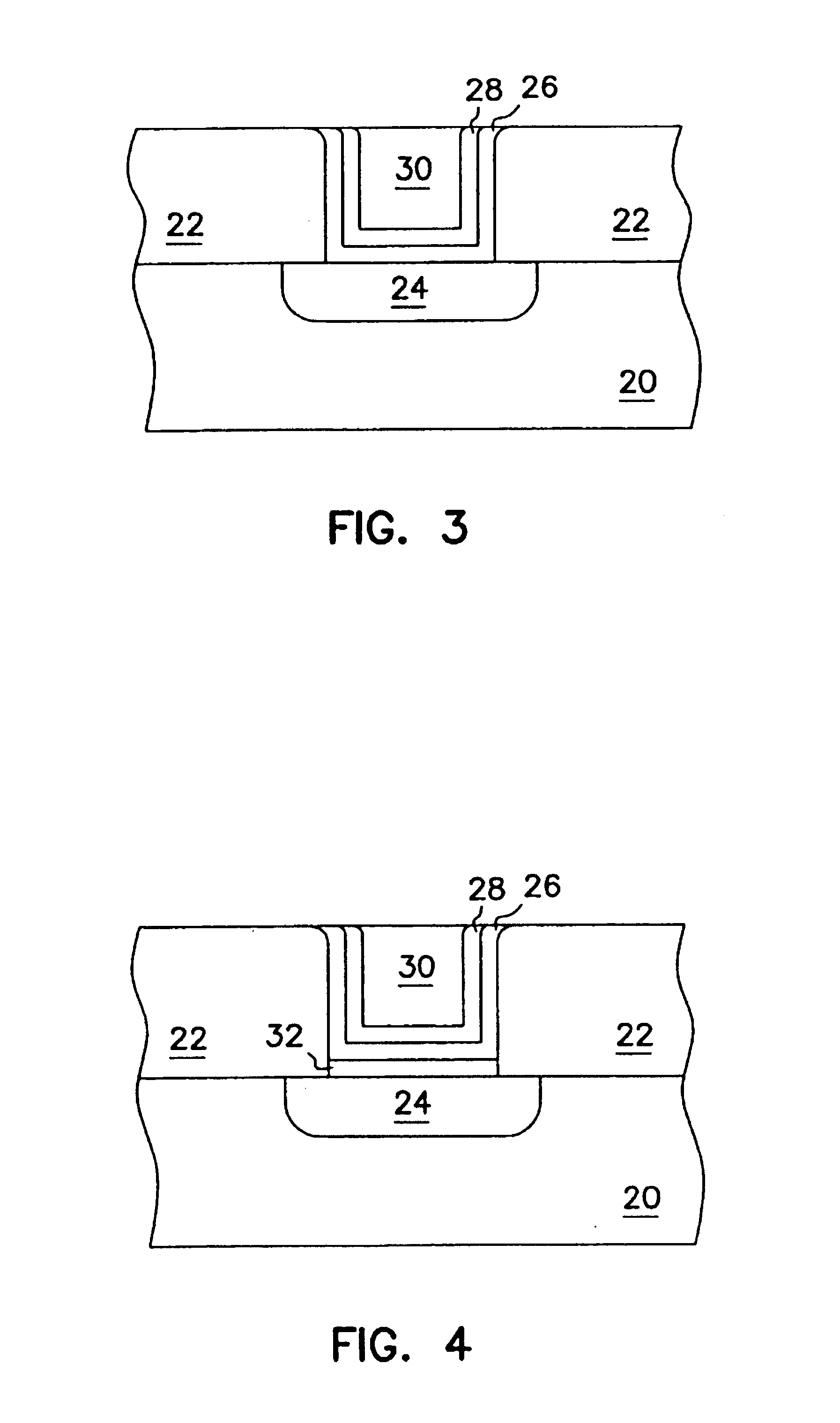
[0017]In the following detailed description of the preferred embodiments, reference is made to the accompanying drawings which form a part hereof, and in which is illustrated by way of specific embodiments in which the invention may be practiced. It is to be understood that other embodiments may be utilized and that structural or logical changes may be made without departing from the scope of the present invention. For example, the terms wafer and substrate used in the following description include any semiconductor-based structure. Wafer and substrate are used interchangeably to refer to supporting semiconductor structures 20 during processing, as illustrated in FIGS. 1 to 4. Both are to be understood as including silicon-on-sapphire (SOS) technology, silicon-on-insulator (SOI) technology, doped and undoped semiconductors, epitaxial layers of a silicon supported by a base semiconductor, as well as other semiconductor structures well known to one skilled in the art. Furthermore, whe...


PUM

PropertyMeasurementUnit
grain sizeaaaaaaaaaa
thicknessaaaaaaaaaa
thicknessaaaaaaaaaa

Abstract

A first layer of titanium nitride (TiN) is formed on a semiconductor structure, such as an interconnect via. Then, a second layer of TiN is formed on the first layer of TiN. The first layer of TiN is amorphous. The second layer of TiN is polycrystalline, having a mixed grain orientation. Finally, an aluminum film is formed on the second layer of titanium nitride. Optionally, a titanium silicide layer is formed on the semiconductor structure prior to the step of forming the first layer of titanium nitride. Interconnects formed according to the invention have polycrystalline aluminum films with grain sizes of approximately less than 0.25 microns.

Description

[0001]This application is a Divisional of U.S. application Ser. No. 09 / 146,509, filed Sep. 3, 1998 now U.S. Pat. No. 6,187,673.FIELD OF THE INVENTION[0002]The present invention relates generally to semiconductor integrated circuits and methods for their fabrication and, more particularly, to aluminum interconnects and methods for their formation.BACKGROUND[0003]Semiconductor integrated circuits (ICs) contain individual devices, which are typically operatively-coupled together using metal lines. In most applications, the metal lines are formed on a different level than the devices, separated by an intermediate dielectric, such as silicon oxide or borophosphosilicate glass (BPSG). The most commonly used metal lines are aluminum. Interconnects are formed between individual devices and the metal lines. A typical interconnect between metal layers is composed of a via (i.e. opening) formed in an intermediate dielectric. Similarly, an interconnect between a metal layer and silicon is compo...

Claims


Application Information

Patent Timeline
Patent Type & Authority Patents(United States)
IPC IPC(8): H01L21/285H01L21/70H01L21/02H01L21/768
CPCH01L21/28556H01L21/76843H01L21/76846H01L21/76855H01L21/76876H01L21/76877
Inventor LAI, WING-CHEONG GILBERTSANDHU, GURTEJ SINGH
Owner MICRON TECH INC
Why Eureka
Try Eureka