

Small grain size, conformal aluminum interconnects and method for their formation
a technology of aluminum interconnects and conformal aluminum, applied in the direction of semiconductor devices, semiconductor/solid-state device details, electrical apparatus, etc., can solve the problems of difficult to obtain adequate step coverage, non-conformal layers, and unsatisfactory interconnects, so as to improve the ohmic characteristics of the contact, diffuse easily through the interconnect structure, and reduce the resistance contact
Patent Information
- Authority / Receiving Office
- US · United States
- Patent Type
- Applications(United States)
- Current Assignee / Owner
- Publication Date
- 2005-01-13
- Estimated Expiration
- Not applicable · inactive patent
Smart Images
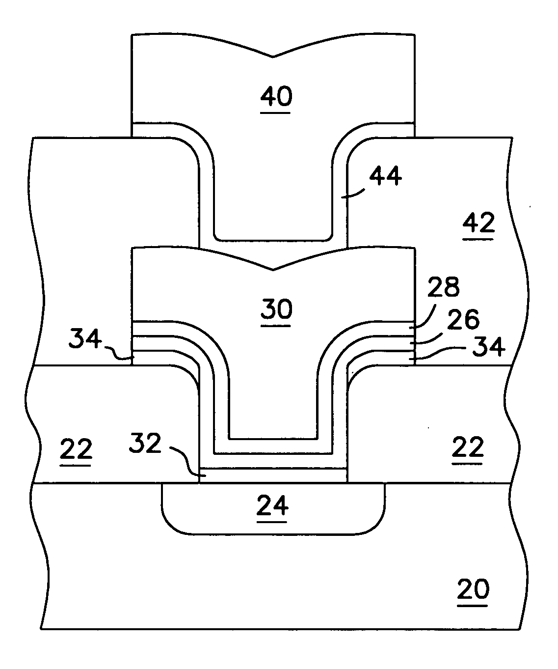
Figure 1 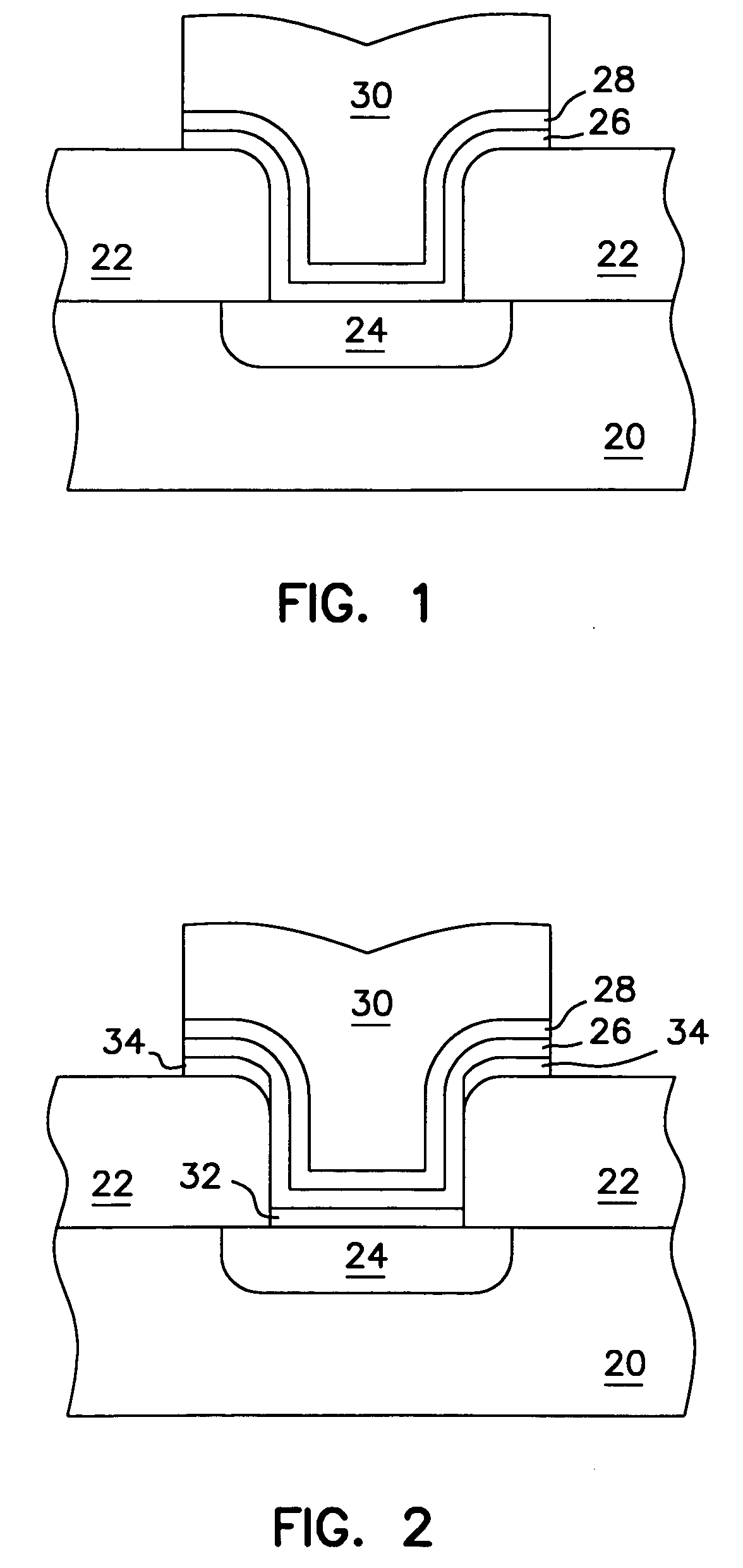
Figure 2 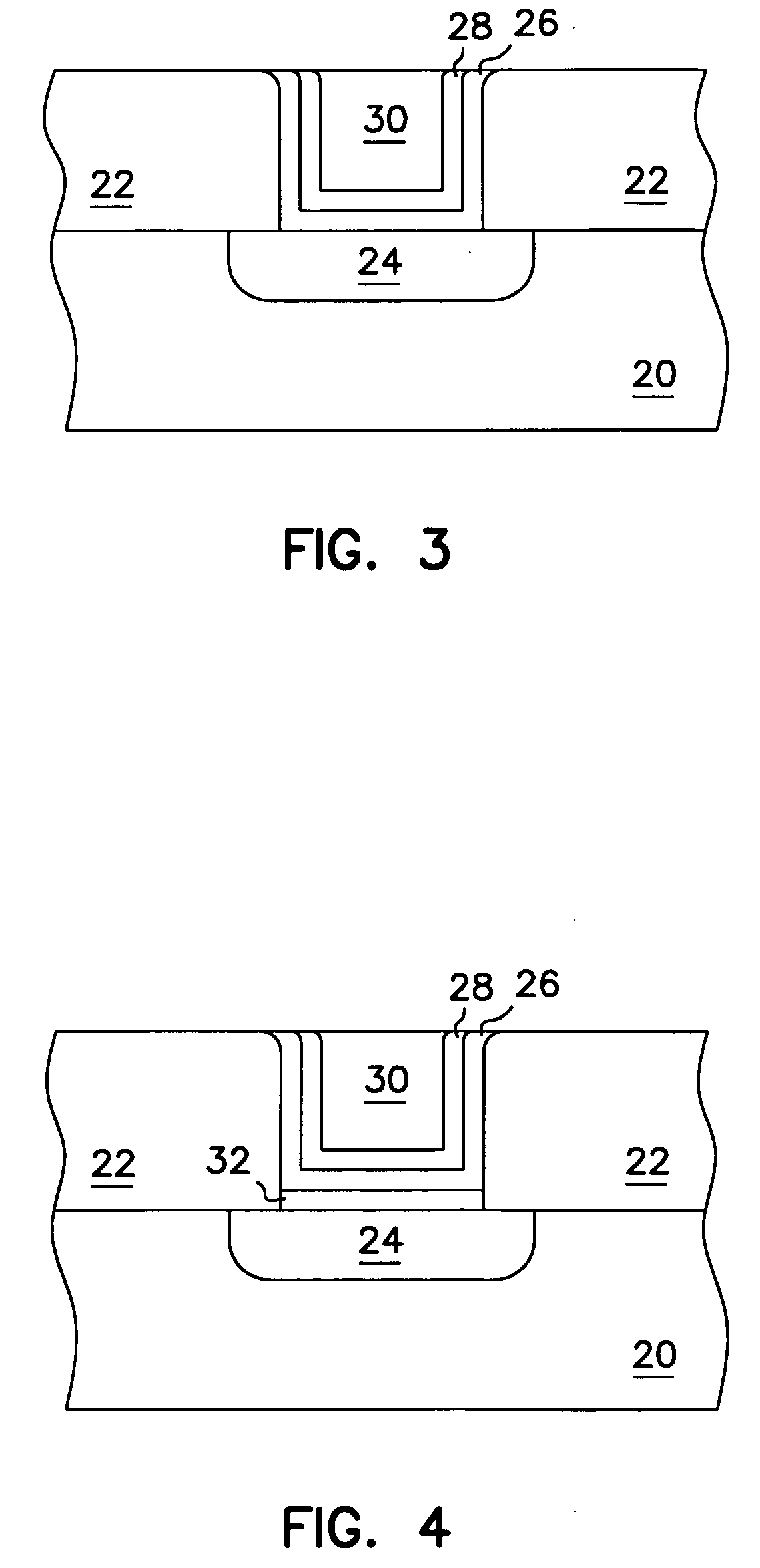
Figure 3
Abstract
Description
[0001] This application is a Divisional of U.S. application Ser. No. 09 / 782,498, filed Feb. 13, 2001, which is a Divisional of U.S. application Ser. No. 09 / 146,509, filed Sep. 3, 1998, now U.S. Pat. No. 6,187,673, both of which are herein incorporated by reference.FIELD OF THE INVENTION
[0002] The present invention relates generally to semiconductor integrated circuits and methods for their fabrication and, more particularly, to aluminum interconnects and methods for their formation. BACKGROUND
[0003] Semiconductor integrated circuits (ICs) contain individual devices, which are typically operatively-coupled together using metal lines. In most applications, the metal lines are formed on a different level than the devices, separated by an intermediate dielectric, such as silicon oxide or borophosphosilicate glass (BPSG). The most commonly used metal lines are aluminum. Interconnects are formed between individual devices and the metal lines. A typical interconnect between metal layers ...
Examples
Embodiment Construction
[0017] In the following detailed description of the preferred embodiments, reference is made to the accompanying drawings which form a part hereof, and in which is illustrated by way of specific embodiments in which the invention may be practiced. It is to be understood that other embodiments may be utilized and that structural or logical changes may be made without departing from the scope of the present invention. For example, the terms wafer and substrate used in the following description include any semiconductor-based structure. Wafer and substrate are used interchangeably to refer to supporting semiconductor structures 20 during processing, as illustrated in FIGS. 1 to 4. Both are to be understood as including silicon-on-sapphire (SOS) technology, silicon-on-insulator (SOI) technology, doped and undoped semiconductors, epitaxial layers of a silicon supported by a base semiconductor, as well as other semiconductor structures well known to one skilled in the art. Furthermore, wh...