Light source

a technology of light source and led die, which is applied in the direction of printed circuit parts, printed circuit non-printed electric components association, printed element electric connection formation, etc., can solve the problems of the package not being able to operate at higher power, the heat dissipation rate of the conductive interconnect is severely limited, and the heat dissipation rate is not high enough to prevent the package from detaching easily, and the thermal path length is minimised. , the effect of efficient hea

Inactive Publication Date: 2005-09-27
DOCUMENT SECURITY SYST
View PDF18 Cites 76 Cited by
  • Summary
  • Abstract
  • Description
  • Claims
  • Application Information

AI Technical Summary

Benefits of technology

[0011]In a preferred embodiment, the platform extends over the first surface and over the side wall of the substrate. This has the advantage of holding the platform firmly in place on the substrate, thus preventing it from detaching easily.
[0012]Suitably, the platform is made from a thermally conductive material such as metal for conducting heat away from the light emitting diode, and is configured such that a first surface faces the aperture on which the light emitting diode is mounted, and an opposite second surface is exposed on the outside of the light source. Consequently, the thermal path is provided from the first surface of the platform to the second surface of the platform. Advantageously, the distance from the first surface to the second surface of the platform may be minimised to minimise the length of the thermal path and make it more efficient at dissipating heat.
[0013]A light source in accordance with the invention also has the advantage that by mounting the light emitting diode in the aperture of the substrate the package occupies a smaller volume.

Problems solved by technology

A drawback with the LED package of FIG. 1 is its inefficiency in dissipating heat away from the LED die 110.
However, the rate of heat dissipation from the conductive interconnects is severely limited by i) the small cross-sectional area of the interconnects, and ii) the relatively large distance of the heat path offered by the interconnects.
The poor heat dissipation properties of the LED package of FIG. 1 limit the ability of the package to operate at higher power and thus increased brightness.
Without efficient heat dissipation, the increased power supplied to the package rapidly increases the temperature of the die resulting in poor light extraction efficiency and even permanent damage to the die.

Method used


Image

  • Light source
  • Light source
  • Light source

Examples


Embodiment Construction

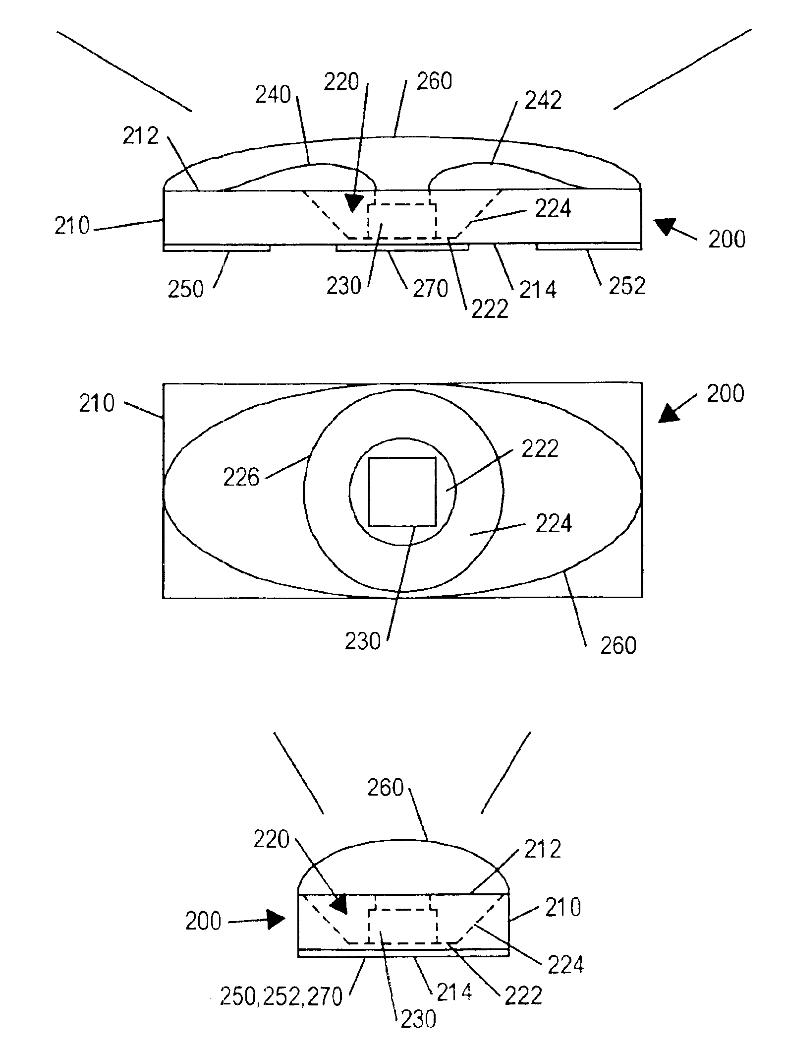
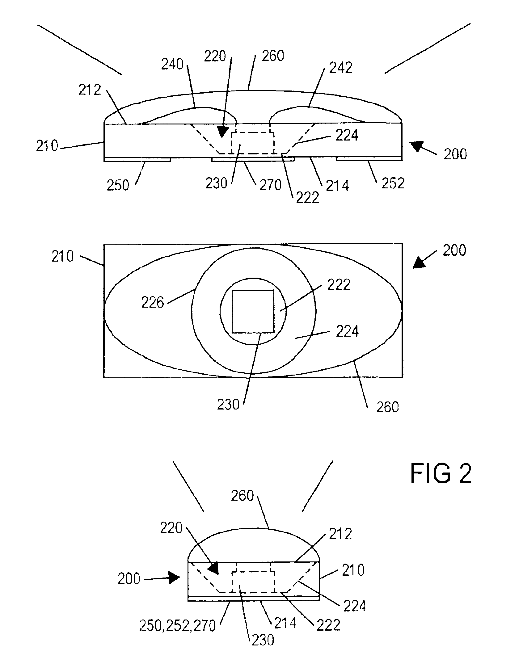
[0025]Referring to FIG. 2, there is shown schematically an LED package 200 which can be surface mounted onto a printed circuit board by, for example, reflow soldering or possibly manual soldering.

[0026]The surface mount LED package 200 includes a rectangular planar substrate 210, such as an epoxy or glass laminate, a polyester or polyamide board, a bismaleimidetraizine (BT) resin board, or a thermosetting polyphenylene ether board. An upper surface 212 of the substrate includes a conic-section shaped recess 220 positioned centrally on the upper surface. The recess 220 comprises a generally circular floor 222, and a curved side wall 224 tapering concentrically outwards from the floor towards a circular edge 226 on the upper surface 212.

[0027]The light emitting element of the LED package 200 is provided by a light emitting diode (LED) die 230 which is mounted centrally in the recess 220 of the substrate 210. As illustrated in the front view of the LED package, two thin gold wires 240,...


PUM


Abstract

A light source suitable for surface mounting onto a printed circuit board. The light source includes a planar substrate with a centrally positioned aperture. A light emitting diode is mounted on a metallic layer covering the bottom of the aperture, and is encapsulated by a transparent encapsulant material. The metallic layer provides a thermal path for heat generated by the light emitting diode.

Description

BACKGROUND OF THE INVENTION[0001]This invention relates to a light source. In particular, the invention relates to a high-power light source in the form of a light emitting diode (LED) package.[0002]Light emitting diodes (LEDs) fabricated from silicon wafer are commonly used to generate light in a variety of applications ranging from simple low-power indication lights to higher-power LED traffic light clusters and LED matrix video displays. Typically, the light emitting diode die is assembled into a sealed package containing electrical connections between the die and terminal pads exposed on an outer surface of the package. Such a package enables simple connection of the diode to external circuitry and, due the sealing properties of the package, protects the die from external damage.[0003]Recently, there has been a drive to make smaller surface mount LED packages which allow the LED to be reliably mounted onto a printed circuit board substrate at relatively high speeds. By making in...

Claims


Application Information

Patent Timeline
Patent Type & Authority Patents(United States)
IPC IPC(8): H01L33/00H05K3/40H05K3/00H05K3/42H05K1/18H01L33/54H01L33/56H01L33/60H01L33/62H01L33/64
CPCH01L33/486H01L33/642H05K3/403H01L33/54H05K1/183H05K3/0052H05K3/42H05K2201/0394H01L2224/48091H01L2224/48227H01L2924/00014H05K2201/10106H01L2224/45144H01L2924/00H01L2924/10253H01L2924/3025
Inventor YOGANANDAN, SUNDAR A/L NATARAJANLIM, SEONG CHOON
Owner DOCUMENT SECURITY SYST
Why Eureka
Try Eureka