System and method of providing highly isolated radio frequency interconnections

a radio frequency interconnection and highly isolated technology, applied in the direction of waveguides, non-printed jumper connections, waveguide type devices, etc., can solve the problems of microstrips being subject to emi from nearby conductors, coaxial cables utilized as isolated interconnection transmission lines are not compatible with automated smt assembly process, and soldering at a much greater cos

Inactive Publication Date: 2005-09-27
INTEL CORP
View PDF32 Cites 24 Cited by
  • Summary
  • Abstract
  • Description
  • Claims
  • Application Information

AI Technical Summary

Problems solved by technology

Coaxial cable utilized as an isolated interconnecting transmission line is not compatible with the automated SMT assembly process flow and generally must be hand formed and soldered at a much greater expense.
Microstrip is also subject to EMI from nearby conductors because of its unshielded structure.
1) The multilayer PCB structure exhibits increased thermal resistance from the SMT component side to the reverse side which is commonly attached to a heatsink.
2) In practice, the two ground planes are conventionally connected together along two paths parallel to the entire length of the central conducting strip, in order to minimize the difference of potential between the ground planes, and thereby minimize coupling of RF signals between the stripline structure and adjacent circuitry. The ground plane interconnection is normally accomplished with conductive through-holes, thereby adding significant cost to the final PCB assembly.
3) PCB material handling and processing costs are much lower when the unpopulated PCB consists of only a back conductive layer, one dielectric layer, and a top SMT compatible layer. Converting the entire PCB to a multilayer PCB structure when only a small number of shielded interconnections are required adds unnecessarily to the final assembly weight, size and cost.
4) Specialized circuit functions including RF power amplifiers are conventionally fabricated on PCB materials, including hard or brittle ceramic substrates, that are not compatible with multilayer PCB fabrication techniques, thereby precluding the inclusion of stripline as an inherent part of the unpopulated PCB.

Method used


Image

  • System and method of providing highly isolated radio frequency interconnections
  • System and method of providing highly isolated radio frequency interconnections
  • System and method of providing highly isolated radio frequency interconnections

Examples


first embodiment

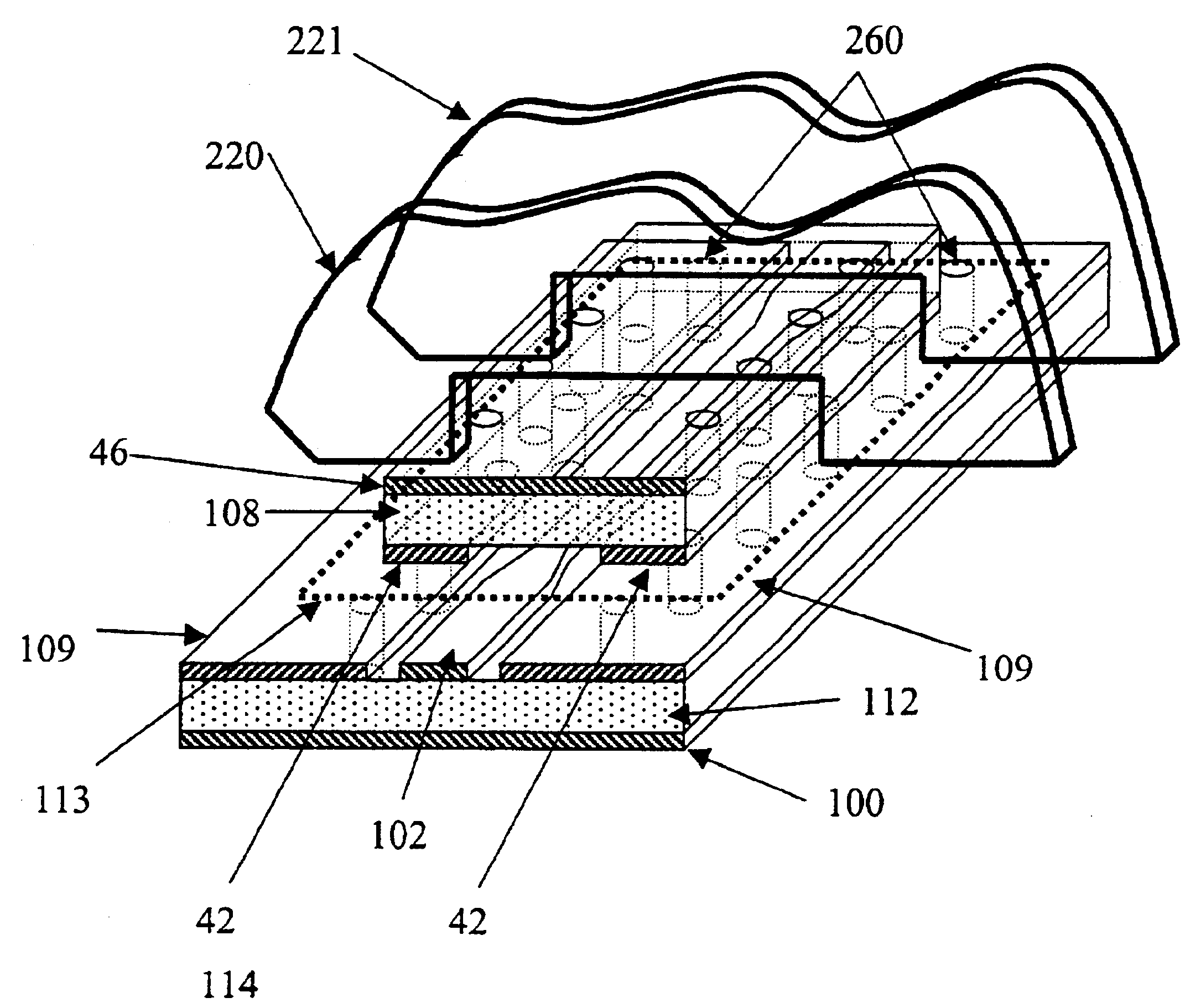
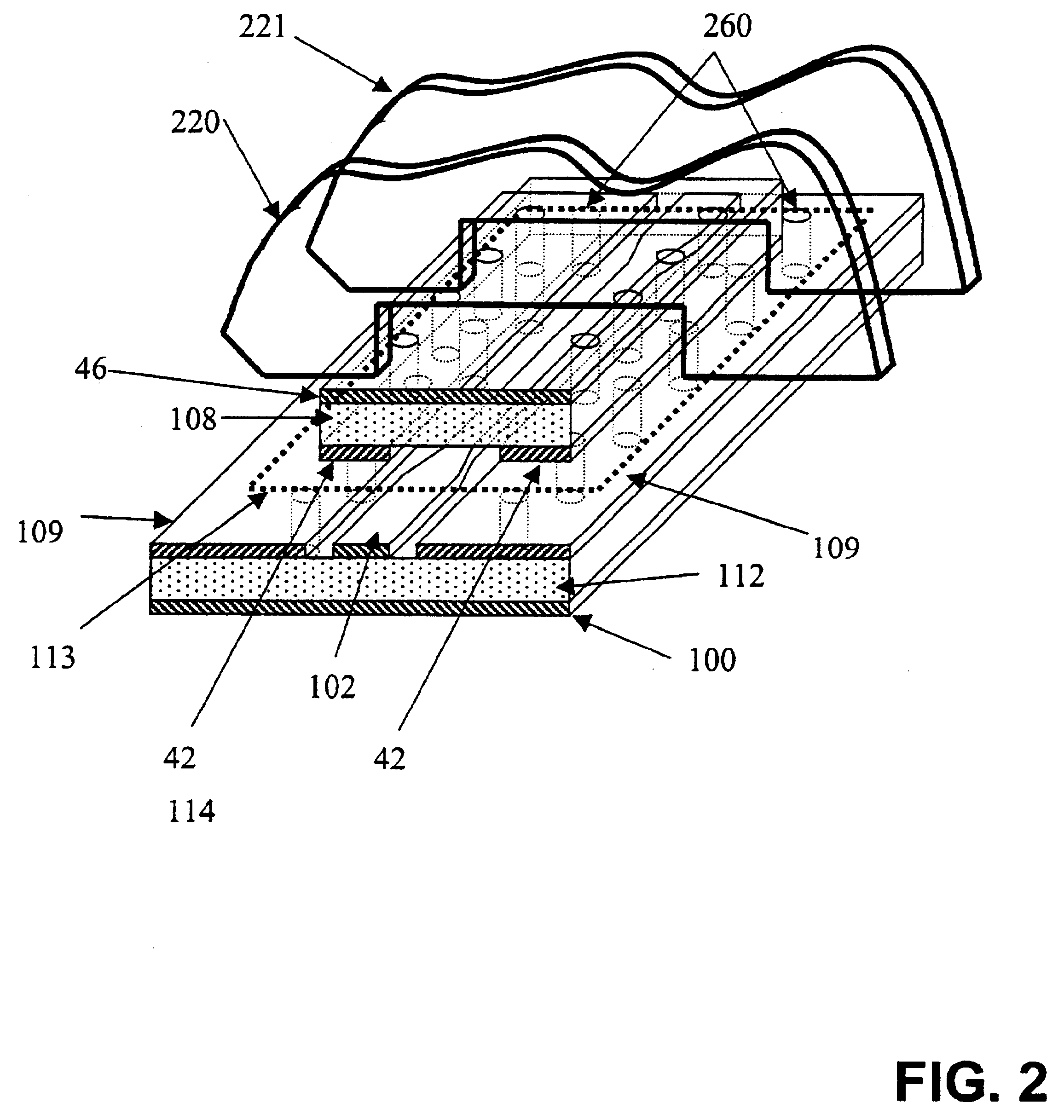
[0037]In the invention a fully shielded interconnection between shielded cavities 220, 221 is provided. The SMT component 108 when applied to a printed wiring assembly having a conductive pattern 113 appropriate to form part of a stripline structure may be utilized to form a completely shielded interconnection between a first 220 and a second 221 shielded cavity. The completely shielded interconnection is formed from the printed wiring board by virtue of the conductive pattern, functioning in conjunction with the SMT part disposed on the printed wiring board.

[0038]The SMT component 108 is attached to the base PCB 115 so that conductive layers 42 and 113 are substantially aligned and in electrical contact. One or more grounded isolating walls 220, 221 surround and are in electrical contact with the top layer 46 of the SMT component 108, thereby minimizing EMI between the SMT structure and surrounding circuit blocks or structures shielded, and further minimizing EMI between separate c...

second embodiment

[0046]In the conductive area 113, the locations of the multiple conductive plated through holes 260 fall outside of the outline of the SMT part, but are close enough to it to still provide sufficient grounding and a good solder joint. Solder wicking as described above can be prevented by selectively applying an optional pattern or layer of solder resisting film (not shown) over holes 260, using methods known to those skilled in the art.

[0047]FIG. 5 is a side cross-section view of the attachment of the SMT component to the printed wiring assembly and to the shield assembly. As shown shields 220,221 are coupled to The SMT component, which is in turn coupled to the base PCB 115 that includes the conductive pattern.


PUM


Abstract

A surface mount technology (“SMT”) apparatus for use in routing radio frequencies (“RF”) between cavities that require a high level of isolation on a single printed circuit board (“PCB”). The SMT part is attached to the PCB over a stripline-ready trace which transitions to microstrip before and after the SMT stripline part to maintain consistent characteristic impedance. When presented with a high isolation need between two cavities using microstrip transmission lines, the proposed stripline SMT apparatus under the isolation wall will tend to provide the necessary isolation. The present invention provides a repeatable and reliable interconnect while improving the electrical match between the two cavities. Furthermore, the invention removes the costs associated with manually forming and soldering cables between PCBs.

Description

BACKGROUND OF THE INVENTION[0001]The present invention relates generally to radio frequency (“RF”) and electromagnetic interference (“EMI”) protection for electronic circuitry, and in particular, to a surface mount technology (“SMT”) stripline structure used in combination with an isolation wall for routing radio frequencies between two cavities that require a high level of isolation.[0002]Printed circuit boards (“PCB”) comprise a dielectric substrate which supports the printed wiring, including both circuit and ground traces. The detailed method of construction of printed circuit board and the materials used are well known in the art. Many PCBs require a means of signal isolation to reduce or prevent RFI and EMI between various groups or blocks of circuitry. The circuit blocks comprise both active and passive components. In accordance with conventional SMT practice, these electrical components are mounted on the top surface of the printed circuit board during the automated (“compon...

Claims


Application Information

Patent Timeline
Patent Type & Authority Patents(United States)
IPC IPC(8): H01P3/08H01P5/08H01P1/04H05K1/02H05K3/22
CPCH01P1/047H01P3/081H01P3/085H01P5/08H05K1/0243H05K1/0219H05K3/222H05K2201/0715H05K2201/09618H05K2201/09727
Inventor SWEENEY, RICHARDSNODGRESS, JASON
Owner INTEL CORP
Why Eureka
Try Eureka