Semiconductor substrate and process for its production

a technology of semiconductors and substrates, applied in the field of semiconductor substrates, can solve the problems of complicated and laborious setting conditions, rendering the reading of marks difficult, etc., and achieve the effect of easy marking

Inactive Publication Date: 2005-10-11
CANON KK
View PDF29 Cites 22 Cited by
  • Summary
  • Abstract
  • Description
  • Claims
  • Application Information

AI Technical Summary

Benefits of technology

[0019]An object of the present invention is to provide a semiconductor substrate which has a readable mark and can be easily marked without causing deposition of splashed particles, and to provide also a process for producing the semiconductor substrate.

Problems solved by technology

The conditions of not causing the splashing of particles depend on the SOI layer structure and the thickness of the respective layers, so that the setting conditions therefor are complicated and laborious.
Furthermore, when the laser has a lower output level that the particle splashing is retarded, the depth of the recessed portion formed by the laser irradiation becomes smaller, thereby rendering the reading of the mark difficult.

Method used


Image

  • Semiconductor substrate and process for its production
  • Semiconductor substrate and process for its production
  • Semiconductor substrate and process for its production

Examples


embodiment 1

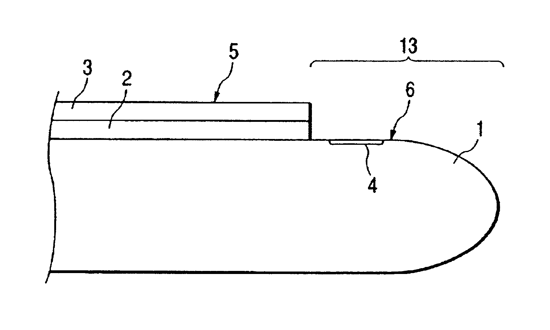
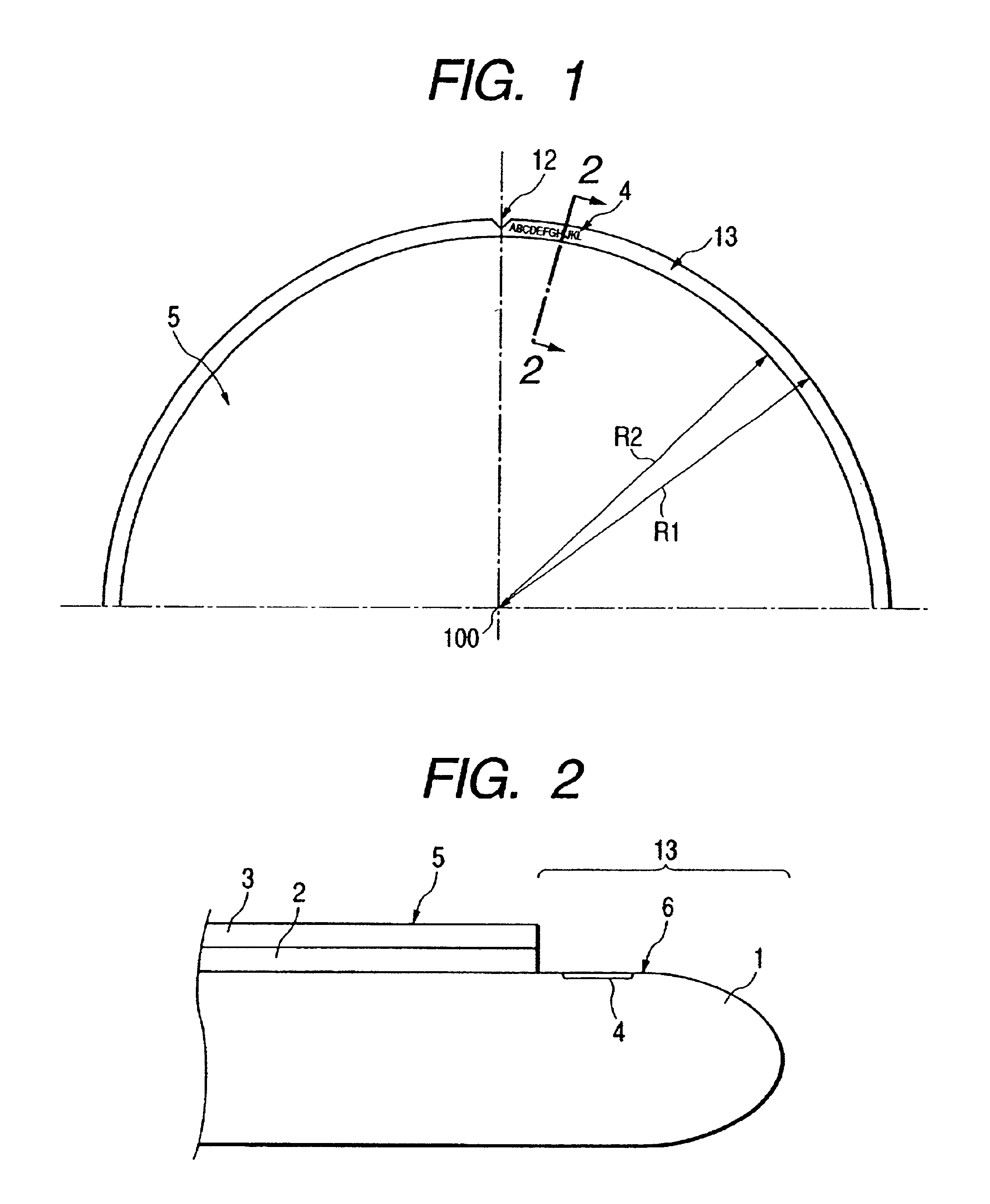
[0048]FIG. 1 is a top view of a part of a semiconductor substrate according to the present invention. FIG. 2 is a cross-sectional view of the semiconductor substrate taken along the line 2—2 of FIG. 1.

[0049]An SOI substrate is constituted of a supporting substrate 1 such as a single-crystalline silicon wafer, a buried insulating layer 2 such as of silicon oxide, and a semiconductor layer (SOI layer) 3 such as a single-crystalline silicon layer.

[0050]In a surface region 5 of the semiconductor layer 3, a semiconductor device for an integrated circuit and the like is formed. A mark 4 is formed in a region 6 which is a nearly flat region of the surface of peripheral region 13 of the semiconductor substrate. The substrate has a notch 12.

[0051]The edge of the surface region 5 of the SOI layer 3 (i.e., inside border line of the peripheral region) is indicated by the circle of a radius R2. The outer peripheral edge (outside border line of the peripheral region) of the substrate is indicated...

embodiment 2

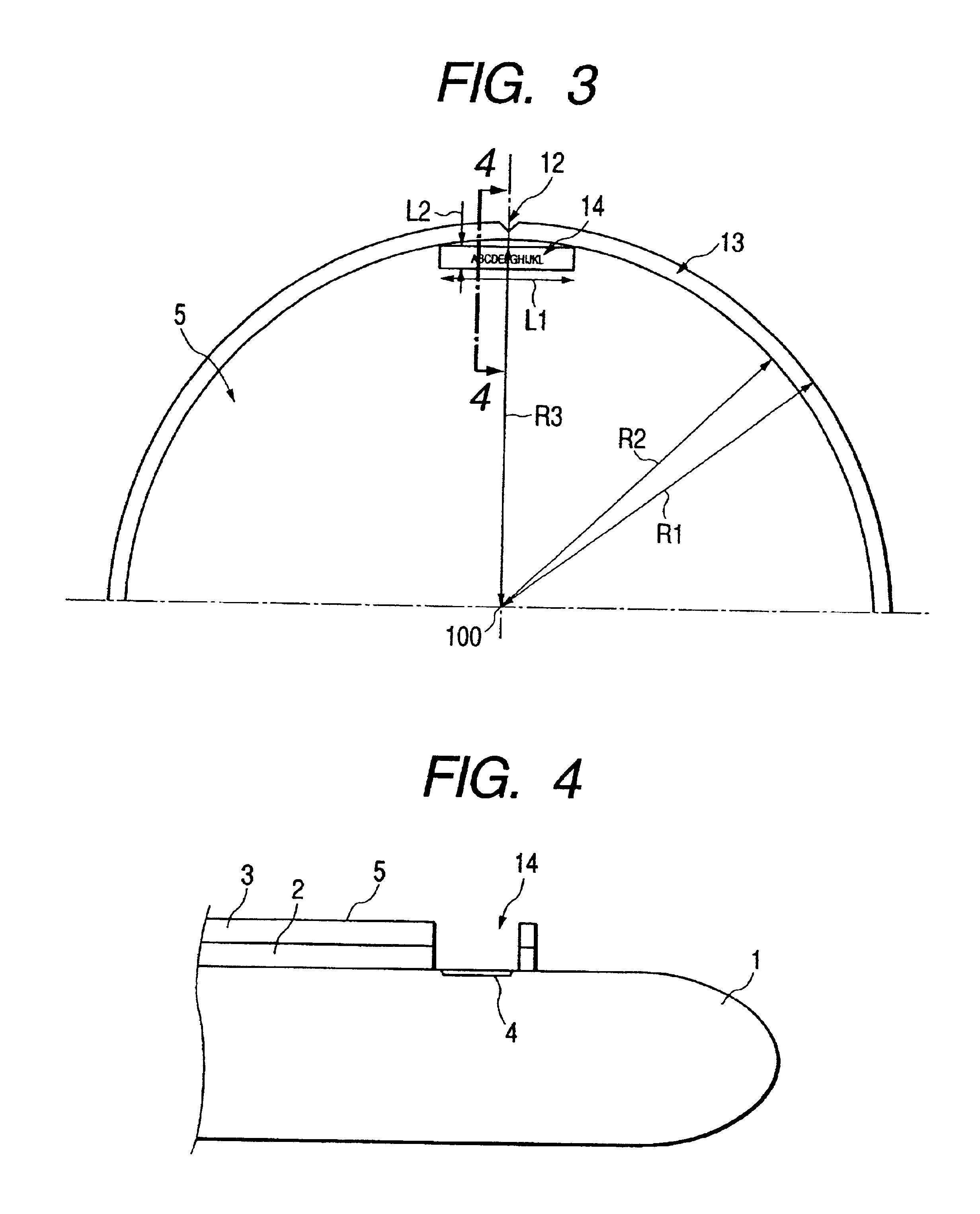
[0056]FIG. 3 is a top view of a part of a semiconductor substrate according to the present invention. FIG. 4 is a cross-sectional view of the semiconductor substrate taken along the line 4—4 of FIG. 3.

[0057]A semiconductor layer (SOI layer) 3 and a insulating layer 2 are partially hollowed and removed to form an exposed region 14, where a part of the supporting substrate 1 is exposed, inside the edge of the semiconductor layer 3, namely on a region (internal region) excluding the peripheral region 13 from the supporting substrate 1.

[0058]The mark 4 is made on this exposed region 14. Although in FIG. 3 the mark 4 is constituted of alphabets, the mark 4 may be a bar code, a numeral, a character, a symbol, or combination thereof.

[0059]The edge (inside border line of the peripheral region) of the surface region 5 of the SOI layer 3 is shown by a circle line of radius R2. The outer peripheral edge (outside border line of the peripheral region) of the substrate is shown by the circle of a...

embodiment 3

[0061]In this Embodiment, the mark is formed on the back surface of the supporting substrate.

[0062]In this Embodiment, the mark is formed on the back surface of a supporting substrate of the SOI substrate in the same manner as the marking on the front surface of a mirror wafer as shown in FIGS. 19 and 20.

[0063]Since the mark is made on the back surface of the supporting substrate, the effective area of the SOI layer on the front surface of the supporting substrate is not decreased.


PUM


Abstract

The present invention provides a semiconductor substrate comprising a semiconductor layer 3 formed on a supporting substrate 1 with interposition of an insulating layer 2 therebetween, wherein a mark is formed in a region other than a surface region of the semiconductor layer; and a process for producing the semiconductor substrate.

Description

[0001]This application is a division of application Ser. No. 09 / 749,730, filed Dec. 28, 2000 now abandoned.BACKGROUND OF THE INVENTION[0002]1. Field of the Invention[0003]The present invention relates to a semiconductor substrate for use in production of a semiconductor integrated circuit device such as semiconductor memories, microprocessors, and system LSIs; and a process for production thereof. In particular, the present invention relates to a semiconductor substrate having thereon a mark for identification of the semiconductor substrates and the like, and a process for production thereof.[0004]2. Related Background Art[0005]The semiconductor substrate includes mirror-wafers which are a disk-shaped substrate produced by slicing an ingot and have at least one face polished, and epitaxial wafers constituted of a mirror-wafer and a semicrystalline semiconductor layer formed on the mirror-wafer.[0006]On the other hand, an SOI technique is widely known which forms a single-crystalline...

Claims


Application Information

Patent Timeline
Patent Type & Authority Patents(United States)
IPC IPC(8): H01L23/544H01L21/20
CPCH01L23/544H01L2223/54406H01L2223/54433H01L2223/54493H01L2924/0002H01L2924/00H01L21/20
Inventor SAKAGUCHI, KIYOFUMI
Owner CANON KK
Why Eureka
Try Eureka