Silicon-on-sapphire display with wireless interconnections and method of fabricating same

a liquid crystal display and silicon-on-sapphire technology, applied in non-linear optics, instruments, optics, etc., can solve the problems of limiting the integration of display driving circuitry heretofore to thin film transistors, and fabricating the display on transparent glass or quartz substrates

Inactive Publication Date: 2005-10-11
THE UNITED STATES OF AMERICA AS REPRESENTED BY THE SECRETARY OF THE NAVY
View PDF6 Cites 67 Cited by
  • Summary
  • Abstract
  • Description
  • Claims
  • Application Information

AI Technical Summary

Benefits of technology

[0008]In one aspect of the invention, a liquid crystal display includes: a) a sapphire substrate; b) a single crystal silicon structure disposed on the sapphire substrate to create a silicon-on-sapphire structure; c) a plurality of liquid crystal capacitors disposed on the silicon-on-sapphire structure; d) integrated self-aligned circuitry formed from the crystal silicon structure, where the circuitry modulates the liquid crystal capacitors in response to an input control signal; and e) a receiver disposed on the silicon-on-sapphire structure for receiving electromagnetic radiation and generating the input control signal responsive to the received electromagnetic radiation.
[0009]In another aspect of the invention, a method of fabricating a monolithically integrated crystal array display and control circuitry on a silicon-on-sapphire structure includes the steps of: (a) affixing a single crystal silicon structure to a sapphire substrate; (b) ion implanting the single crystal silicon structure with a species selected from the group consisting of: silicon ions, tin ions, germanium ions, and carbon ions to create an ion-implanted silicon layer; (c) annealing the silicon-on-sapphire structure; (d) oxidizing the ion-implanted silicon layer to form a silicon dioxide layer from a portion of the silicon layer so that a thinned, ion-implanted silicon layer remains; (e) removing the silicon dioxide layer to expose the thinned ion-implanted silicon layer; (f) fabricating transistors wherein each of the transistors is formed by patterning the thinned ion-implan...

Problems solved by technology

Limitations inherent in the existing technology come from the necessity of fabricating the displays on transparent glass or quartz substrates, which are not amenable to high quality electronic materials.
Fabrication of displays on bulk silicon, although of high crystal quality, unnecessarily constrains the display to reflective mode schemes due to the opaque substrate and is not applicable to transmissive applications.
However, the integration of display driving circuitry heretofore has been substantially limited to thin film transistor technology using amorphous (a-Si) or polycrystalline (p-Si) silicon deposited on the glass or quartz substrate.
The intrinsic properties such as lattice and thermal mismatch between the silicon layer and the substrate, and the low temperature deposition techniques used in the a-Si and p-Si technologies result in a silicon layer with poor charge carrier mobility and crystallographic defects.
These limitations are directly related to inferior electron...

Method used


Image

  • Silicon-on-sapphire display with wireless interconnections and method of fabricating same
  • Silicon-on-sapphire display with wireless interconnections and method of fabricating same
  • Silicon-on-sapphire display with wireless interconnections and method of fabricating same

Examples


Embodiment Construction

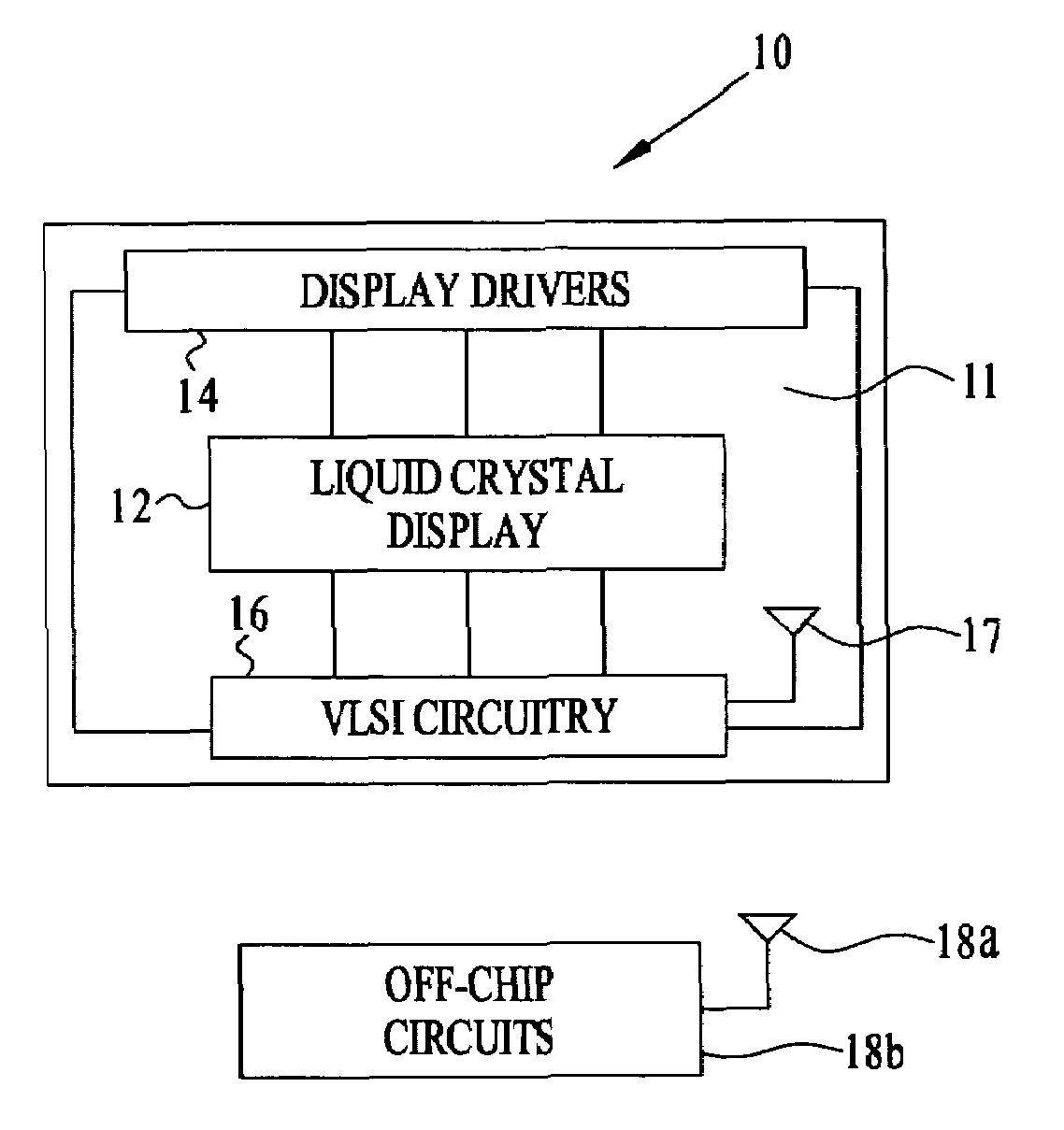
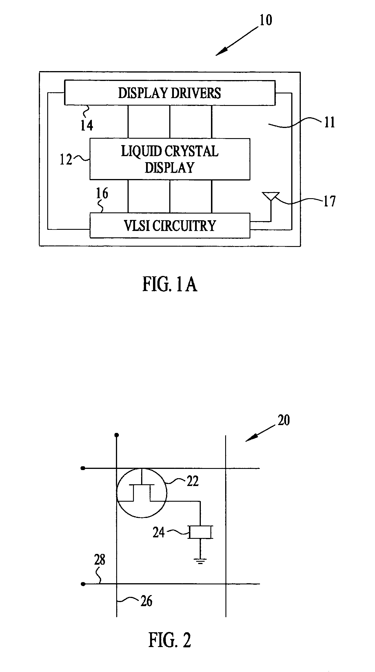
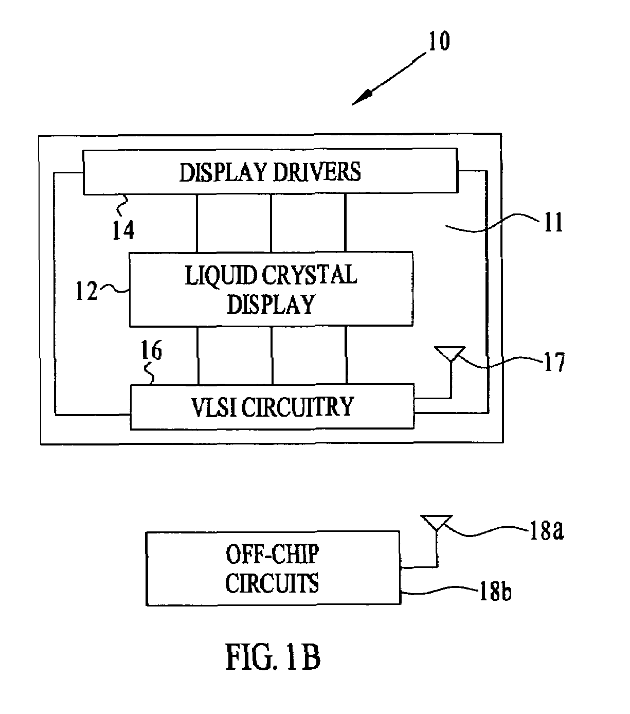
[0018]FIG. 1A shows a SOS display with wireless interconnections 10. Display 10 includes nematic liquid crystal display 12, display drivers 14, very large scale integration (VLSI) circuitry 16, and antenna 17 monolithically integrated on an improved ultra-thin silicon-on-sapphire (UTSOS) wafer 11.

[0019]Liquid crystal display 12 includes an array of one or more pixel elements, which may be individually addressed so that display 12 presents an image for viewing or projection. By way of example, a 1000 pixel×1000 pixel display may be incorporated into display 12, but it is recognized that any number of pixel elements may be utilized as may be necessary to suit the needs of a particular application.

[0020]Display drivers 14 and VLSI circuitry 16 are used to address each of a plurality of individual pixel elements 20 (as shown in FIG. 2) and to generate the appropriate voltages to modulate the liquid crystal capacitors 24 such that a desired image is presented by liquid crystal display 12...


PUM


Abstract

A liquid crystal display includes: a) a sapphire substrate; b) a single crystal silicon structure disposed on the sapphire substrate to create a silicon-on-sapphire structure; c) a plurality of liquid crystal capacitors disposed on the silicon-on-sapphire structure; d) integrated self-aligned circuitry formed from the crystal silicon structure, where the circuitry modulates the liquid crystal capacitors in response to an input control signal; and e) a receiver disposed on the silicon-on-sapphire structure for receiving electromagnetic radiation and generating the input control signal responsive to the received electromagnetic radiation.

Description

CROSS-REFERENCE TO RELATED APPLICATIONS[0001]This application is a continuation-in-part of U.S. patent application Ser. No. 10 / 614,426 (Navy Case No. 84,892) filed Jul. 7, 2003, entitled “Silicon-On-Sapphire Display Apparatus And Method of Fabricating Same,” which is a continuation-in-part of U.S. patent application Ser. No. 09 / 880,660 (Navy Case No. 83,222) filed Aug. 3, 2001, U.S. Pat. No. 6,617,187 entitled “Method For Fabricating An Electrically Addressable Silicon-On-Sapphire Light Valve,” which is a divisional of U.S. patent application Ser. No. 09 / 047,658 (Navy Case No. 79,029) filed Mar. 25, 1998, U.S. Pat. No. 6,312,968 entitled “Method For Fabricating An Electrically Addressable Silicon-On-Sapphire Light Valve,” which is a continuation-in-part of U.S. patent application Ser. No. 08 / 301,170 (Navy Case No. 74,146) filed Sep. 1, 1994 (abandoned), entitled “Method For Fabricating An Electrically Addressable Silicon-On-Sapphire Light Valve,” which is a continuation-in-part of U...

Claims


Application Information

Patent Timeline
IPC IPC(8): G02F1/13G02F1/1343G02F1/1362
CPCG02F1/13454
Inventor RUSSELL, STEPHEN D.SHIMABUKURO, RANDY L.OFFORD, BRUCE W.
Owner THE UNITED STATES OF AMERICA AS REPRESENTED BY THE SECRETARY OF THE NAVY
Why Eureka
Try Eureka