Tunable filter, manufacturing method thereof and optical switching device comprising the tunable filter
a manufacturing method and filter technology, applied in the field of tunable filters, can solve the problems of insufficient performance, inability to increase the number of available wavelengths, and large time and cost, and achieve the effect of quick switching a wavelength and minimizing the crosstalk of adjacent channels
- Summary
- Abstract
- Description
- Claims
- Application Information
AI Technical Summary
Benefits of technology
Problems solved by technology
Method used
Image
Examples
first embodiment
[0047][First Embodiment]
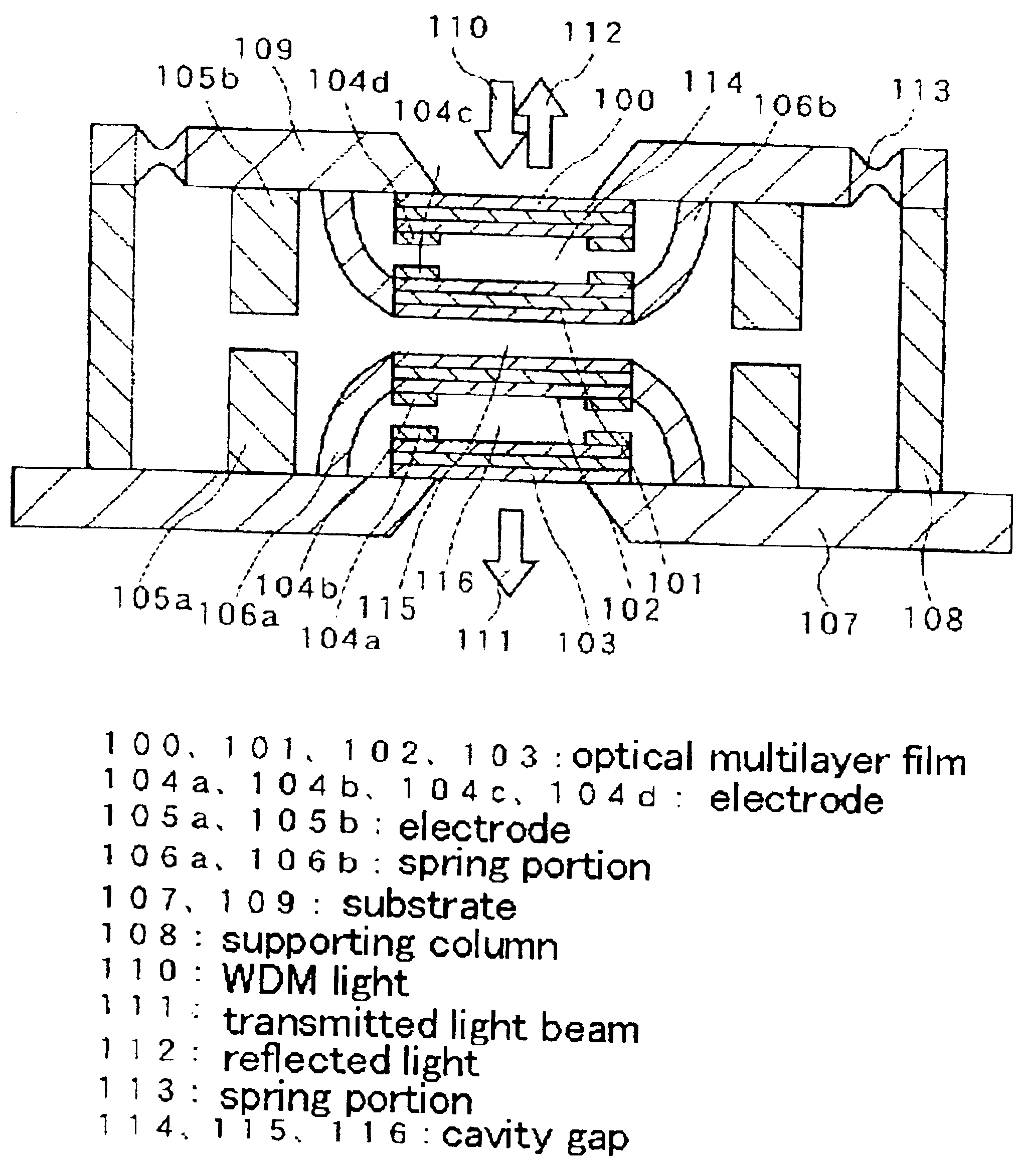
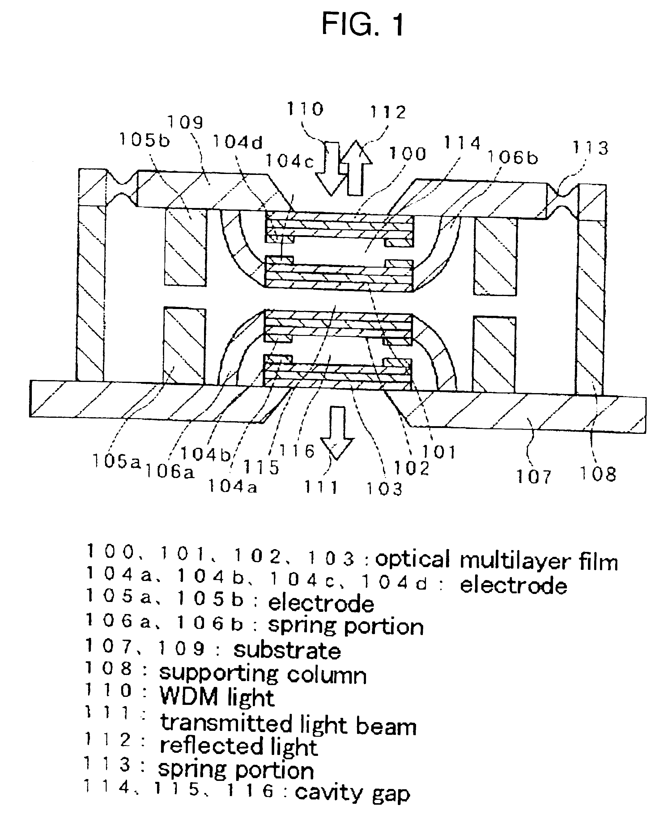
[0048]FIG. 1 is a schematic cross-sectional drawing showing a basic constitution of a tunable filter according to the first embodiment of the invention. In this embodiment, electrostatic drive is adopted for controlling cavity gaps. Manufacturing method of the tunable filter shall be described first, and then the constitution of the tunable filter shall be described. An optical multilayer film 103 is coated on a substrate 107 constituted of a silicon substrate. The optical multilayer film 103 comprises high index films and low index films alternately layered. As the high index film, for example a Ta2O5 film is used, while an SiO2 film is used as the low index film, and these are layered by ion beam deposition for example in 17 layers in total, each having a film thickness of ¼ optical wavelength. Then an Au film is formed in a pattern on the optical multilayer film 103 by sputtering, which is to serve as an electrode 104a.
[0049]And then a polyimide film (not...
second embodiment
[0057][Second Embodiment]
[0058]FIG. 3 is a schematic cross-sectional drawing showing a basic constitution of a tunable filter according to the second embodiment of the invention. In this embodiment, the cavity gaps are controlled by electromagnetic drive. An optical multilayer film 303 is coated on a silicon substrate, which is to serve as substrate 307. The optical multilayer film 303 is formed of high index films and low index films alternately layered. A Ta2O5 film is used as the high index film, and an SiO2 film is used as the low index film, and these are layered by ion beam deposition in 17 layers in total, each having a film thickness of ¼ optical wavelength. Then an Au film is formed in a coil shape, which is to serve as an electromagnet 304a. FIG. 4 shows a coil shape of the electromagnet 304a.
[0059]Then a polyimide film is deposited as a sacrificial layer, to later form a cavity gap 316 by etching on the sacrificial layer. Further on this polyimide film, a Co, Ni or Fe fa...
third embodiment
[0063][Third Embodiment]
[0064]FIG. 5 is a schematic cross-sectional drawing showing a basic constitution of a tunable filter according to the third embodiment of the invention. In this embodiment, the electrostatic drive and the electromagnetic drive are employed in combination to control the cavity gaps. An optical multilayer film 503 is coated on a silicon substrate 507. The optical multilayer film 503 comprises high index films and low index films alternately layered. A Ta2O5 film is used as the high index film, and an SiO2 film is used as the low index film, and these are layered by ion beam deposition in 17 layers in total, each having a film thickness of ¼ optical wavelength. Then an Au film is coated by sputtering, to form an electrode 504a. After that, a polyimide film (not shown) is deposited as a sacrificial layer, to later form a cavity gap 516 by etching on the sacrificial layer. Further on this polyimide film, an Au film is coated by sputtering to form an electrode 504b...
PUM
 Abstract
Description
Claims
Application Information


