
Thin film transistor array substrate and method for manufacturing the same

a technology substrates, which is applied in the direction of transistors, optics, instruments, etc., can solve the problems of a burden on the deterioration of thin film transistors, and the cost of manufacturing materials such as substrates

Inactive Publication Date: 2005-10-18
LG DISPLAY CO LTD
View PDF5 Cites 15 Cited by
  • Summary
  • Abstract
  • Description
  • Claims
  • Application Information

AI Technical Summary

Benefits of technology

The present invention provides a thin film transistor array substrate and a method for manufacturing it that prevents mobile ions from penetrating into a semiconductor layer when using Low End Glass as the substrate. This is achieved by forming a buffer layer on the substrate, doping impurity ions in the buffer layer, and using a phospho-silicate glass layer or a phospho-silicate glass layer with chlorine ions for neutralizing mobile ions. The technical effect is to improve the reliability and performance of the thin film transistor array substrate.

Problems solved by technology

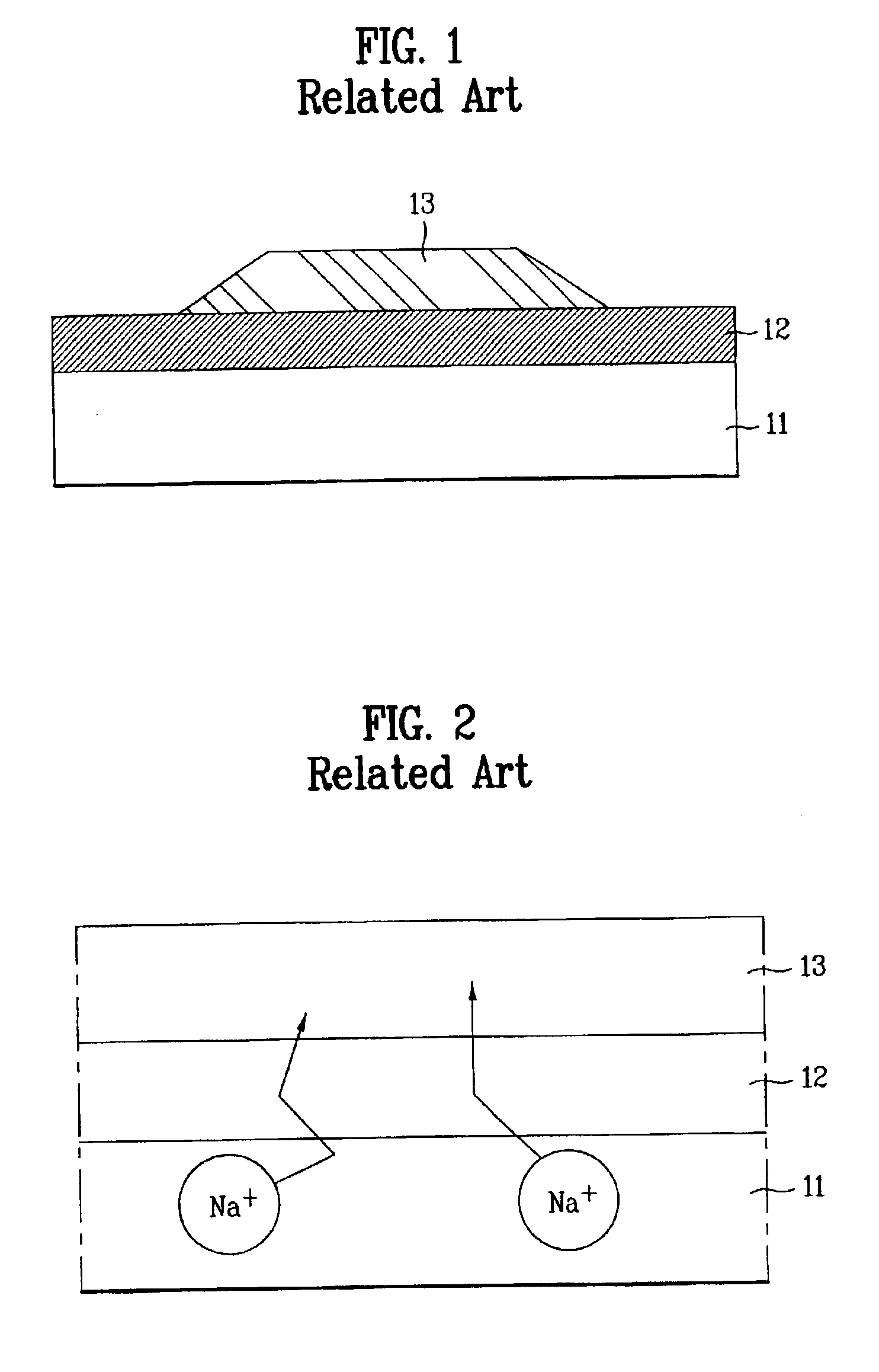
More particularly, the alkaline elements of the transparent glass substrate cause the thin film transistor to deteriorate.
The Alumino-Silicate Glass is three times as expensive as the Soda Lime Glass.
That is, as the size of the LCD device increases, the cost of manufacturing material such as substrate is a burden.
In fact, the amount of mobile ions remaining on the semiconductor layer (a-Si:H, before hardening to a polysilicon) is the most serious problem because the semiconductor layer obtains TFT device characteristics.
However, in case of the active matrix type LCD panel having an amorphous silicon type thin film transistor requiring a high temperature process, it is impossible to use the buffer layer as a barrier layer because the great amount of mobile ions, so the Soda Lime Glass is not used as the substrate in the active type LCD panel.
However, the buffer layer, formed between the semiconductor layer and the substrate, does not serve as a barrier layer, whereby the mobile ions of the substrate may penetrate into the semiconductor layer.

Method used


Image

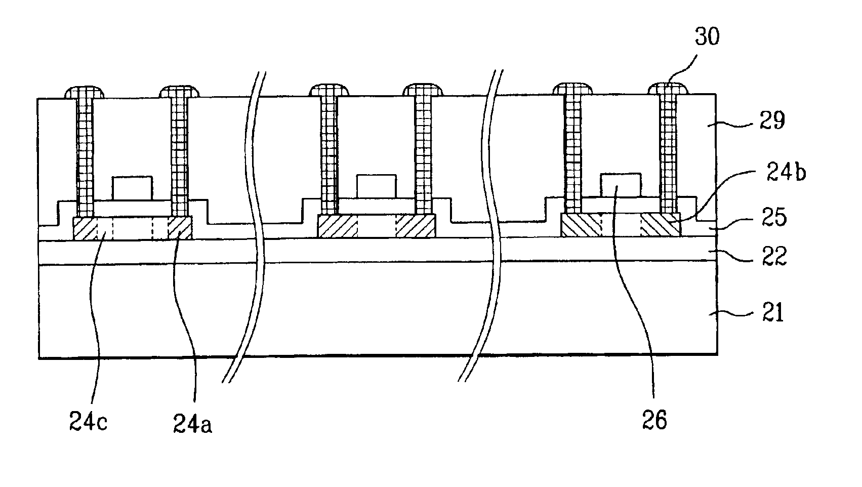
  • Thin film transistor array substrate and method for manufacturing the same
  • Thin film transistor array substrate and method for manufacturing the same
  • Thin film transistor array substrate and method for manufacturing the same

Examples


third embodiment

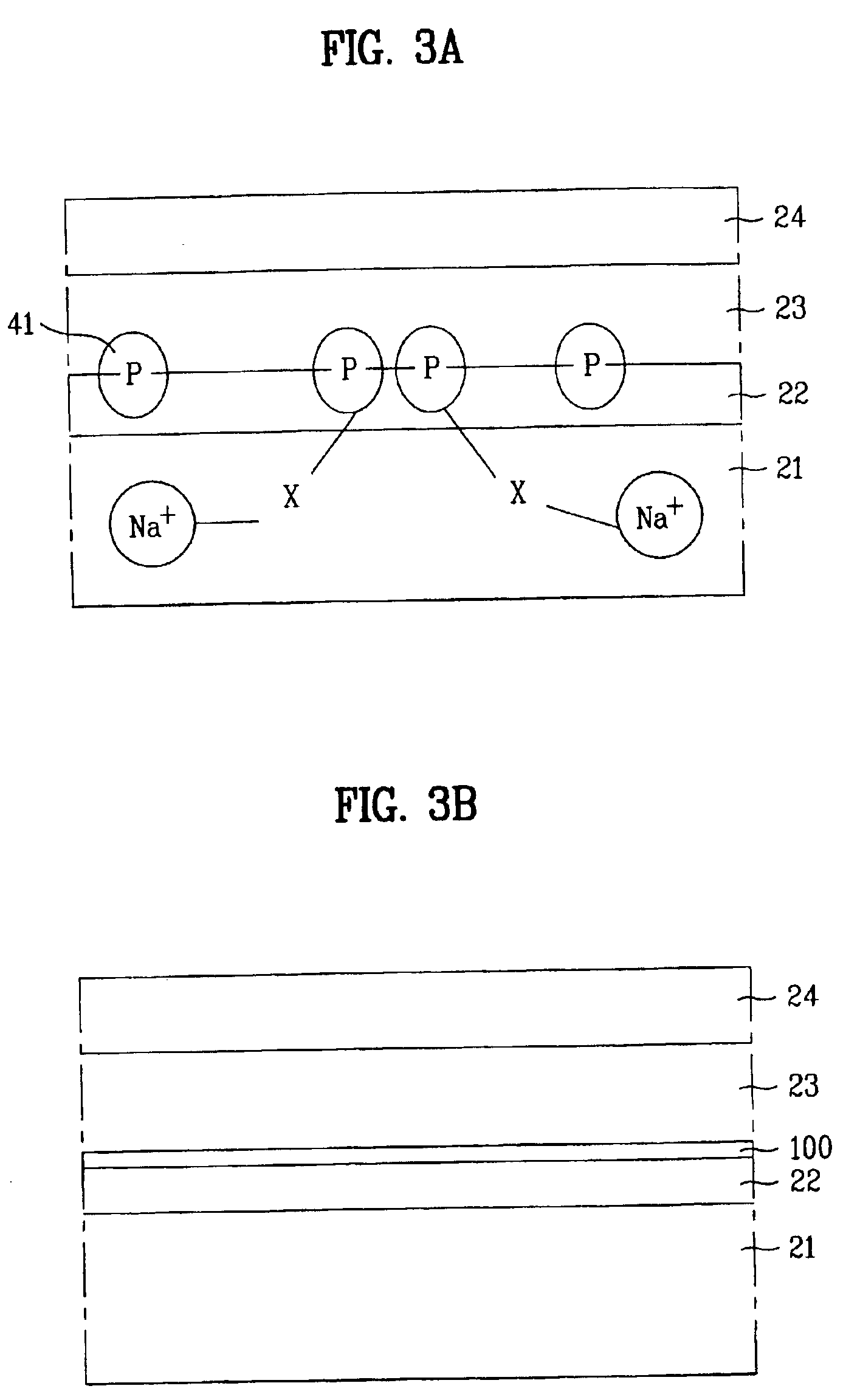
[0052]FIG. 5 is a cross-sectional view schematically illustrating a method for manufacturing a thin film transistor array substrate according to the present invention. The method for manufacturing the thin film transistor array substrate may include the process steps of forming a first buffer layer 520 on a substrate 510 formed of Low End Glass, forming a second buffer layer 530 on the first buffer layer 520, doping an impurity such as phosphorus or chlorine ions on the second buffer layer 530, and forming a pixel electrode (not shown) and a thin film transistor (not shown) having a semiconductor layer 540 on the second buffer layer 530.

[0053]As mentioned above, in the case of doping the phosphorus or chlorine ions after forming the first and second buffer layers 520 and 530, the phosphorous or chlorine ions may distribute throughout the first and second buffer layers 520 and 530 with a Gaussian profile. Accordingly, if the impurity doping process is performed such that the peak of ...

fourth embodiment

[0055]FIG. 6 is a cross-sectional view schematically illustrating a method for manufacturing a thin film transistor array substrate according to the present invention. The method for manufacturing the thin film transistor array substrate includes the process steps of forming a first buffer layer 620 on a substrate 610 formed of Low End Glass, forming an reactive layer 630 on an upper surface of the first buffer layer 620 for preventing mobile ions such as Na and K from moving by performing a plasma treatment using a plasma gas such as phosphorous or chlorine on the upper surface of the first buffer layer 620, forming a second buffer layer 640 on the reactive layer 630, and forming a pixel electrode (not shown) and a thin film transistor (not shown) having a semiconductor layer 650 on the second buffer layer 640.

[0056]When performing the plasma treatment in the upper surface of the first buffer layer 620, the plasma gas including the phosphorous or chlorine penetrates into the first ...

fifth embodiment

[0057]FIG. 7 is a cross-sectional view schematically illustrating a method for manufacturing a thin film transistor array substrate according to the present invention. The method for manufacturing the thin film transistor array substrate may include the process steps of forming a buffer layer 720 on a substrate 710 formed of Low End Glass, doping an impurity such as phosphorous or chlorine ions on the buffer layer 720, and forming a pixel electrode (not shown) and a thin film transistor (not shown) having a semiconductor layer 730 on the buffer layer 720.

[0058]As mentioned above, in case of doping the phosphorous or chlorine ions after forming the buffer layer 720 on the substrate 710, the phosphorous or chlorine ions may distribute throughout the substrate 710 and the buffer layer 720 in a Gaussian profile. Accordingly, if the impurity doping process is performed such that the peak of Gaussian profile is positioned in an interface between the substrate 710 and the buffer layer 720,...


PUM

PropertyMeasurementUnit
temperatureaaaaaaaaaa
weightaaaaaaaaaa

Abstract

A thin film transistor array substrate and a method for manufacturing the same is disclosed, in which it is possible to prevent mobile ions contained in a substrate from penetrating into a semiconductor layer by the gettering effect or neutralization in case soda lime glass is used for the substrate. The method includes forming a buffer layer on a substrate; doping impurity ions in the buffer layer; and forming a pixel electrode and a thin film transistor including a semiconductor layer on the buffer layer.

Description

[0001]This application claims the benefit of the Korean Application Nos. P2002-85735, filed on Dec. 28, 2002 and P2003-24982, filed on Apr. 21, 2003, which are hereby incorporated by reference for all purposes as if fully set forth herein.BACKGROUND OF THE INVENTION[0002]1. Field of the Invention[0003]The present invention relates to a liquid crystal display (LCD) device, and more particularly, to a thin film transistor array substrate and a method for manufacturing the same, in which it is possible to prevent mobile ions contained in a substrate from penetrating into a semiconductor layer by the gettering effect or neutralization in case the substrate is formed of Low End Glass.[0004]2. Discussion of the Related Art[0005]With the development of an information society, demands for various display devices increase. Accordingly, many efforts have been made to research and develop various flat display devices such as liquid crystal displays (LCD), plasma display panels (PDP), electrolu...

Claims


Application Information

Patent Timeline
Patent Type & Authority Patents(United States)
IPC IPC(8): G02F1/13G02F1/1333G02F1/136H01L21/336H01L29/786H01L29/04H01L29/66H01L21/02H01L29/02H01L31/062H01L31/06G02F1/1368G11C19/00H01L21/00H01L21/77H01L21/84H01L27/12H01L29/15
CPCH01L27/1214H01L29/78603H01L27/1218H01L27/1262
Inventor OH, JAE YOUNGNAM, SEUNG HEE
Owner LG DISPLAY CO LTD
Learn More