Silicon carbide power metal-oxide semiconductor field effect transistors having a shorting channel and methods of fabricating silicon carbide metal-oxide semiconductor field effect transistors having a shorting channel

a technology of metal-oxide semiconductor and field effect transistor, which is applied in the direction of semiconductor devices, electrical equipment, basic electric elements, etc., can solve the problems of inability to manufacture vertical sic power mosfets using such techniques, reproducible high inversion layer mobility along the sidewalls of trenches, and inability to achieve high breakdown voltage. , to achieve the effect of reproducible high inversion layer mobility and high breakdown voltag

Inactive Publication Date: 2005-10-18
CREE INC
View PDF72 Cites 109 Cited by
  • Summary
  • Abstract
  • Description
  • Claims
  • Application Information

AI Technical Summary

Problems solved by technology

To make a high current, high voltage, low on-resistance, vertical SiC power MOSFET has, so far, been impractical, at least in part, due to the poor surface mobility of electrons in the inversion layer.
Such anneals may have detrimental impact on the performance of power MOSFETs fabricated using such techniques.
With the Trench MOSFET illustrated in FIG. 1A, however, it may be difficult to achieve a high breakdown voltage and a reproducible high inversion layer mobility along the sidewalls of the trench.
Consequently, the on-resistance may become very high, which may render the structure impractical.
One difficulty with the DIMOSFET structure may be the poor mobility of inversion layer electrons, which can result in a very high on-resistance.
The reduced number of free electrons and the increased scattering may reduce the conduction of current from source to drain, which may result in low effective mobility of electrons and a high on-resistance.
Such research has concluded that lower implant activation temperature (1200° C.) leads to higher electron mobility and higher activation temperature (1400° C.) results in poor electron mobility.
However, the implant activation temperature is typically limited to 1400° C. to avoid surface roughness as indicated before.
However, this is not a high voltage power MOSFET structure.
Unfortunately, this approach suffers from reproducibility.
Several groups, including researches at Rensealar Polytechnic Institute (RPI), Purdue University, and Cree, Inc. have been unsuccessful in their attempts to duplicate this result.
Unfortunately, NO is a health hazard having a National Fire Protection Association (NFPA) health danger rating of 3, and the equipment in which post-oxidation anneals are typically performed is open to the atmosphere of the cleanroom.
They are often exhausted, but the danger of exceeding a safe level of NO contamination in the room is not negligible.
However, Lai et al. concluded that such treatment deteriorates the interface quality which may be improved with a subsequent wet or dry anneal in O2 which may repair the damage induced by nitridation in N2O.
However, this work utilized 6H—SiC and it is not clear whether it would work on 4H—SiC, since many improvements to 6H—SiC MOSFETs have not previously resulted in any significant improvement in 4H—SiC MOSFETs.

Method used


Image

  • Silicon carbide power metal-oxide semiconductor field effect transistors having a shorting channel and methods of fabricating silicon carbide metal-oxide semiconductor field effect transistors having a shorting channel
  • Silicon carbide power metal-oxide semiconductor field effect transistors having a shorting channel and methods of fabricating silicon carbide metal-oxide semiconductor field effect transistors having a shorting channel
  • Silicon carbide power metal-oxide semiconductor field effect transistors having a shorting channel and methods of fabricating silicon carbide metal-oxide semiconductor field effect transistors having a shorting channel

Examples


Embodiment Construction

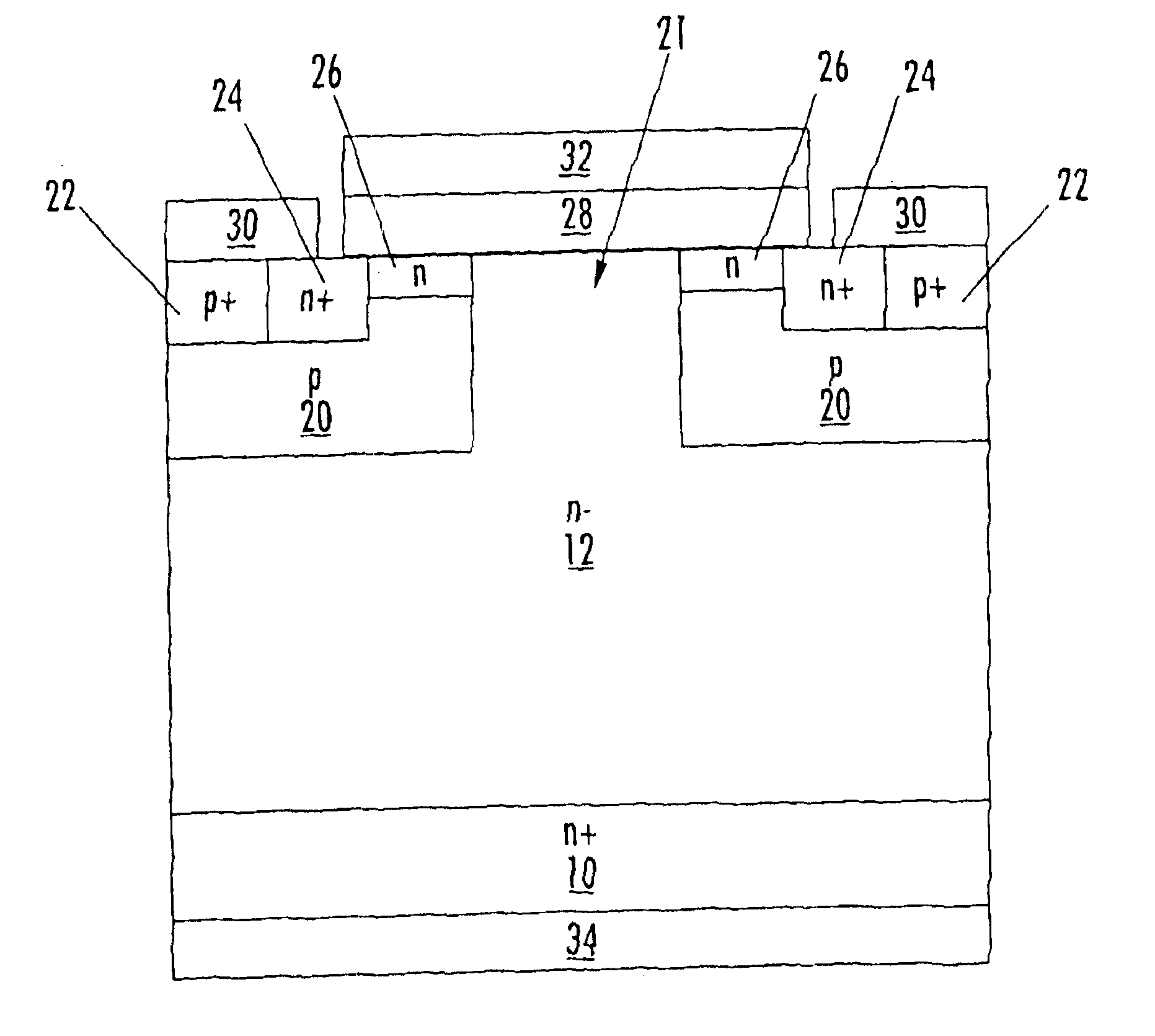
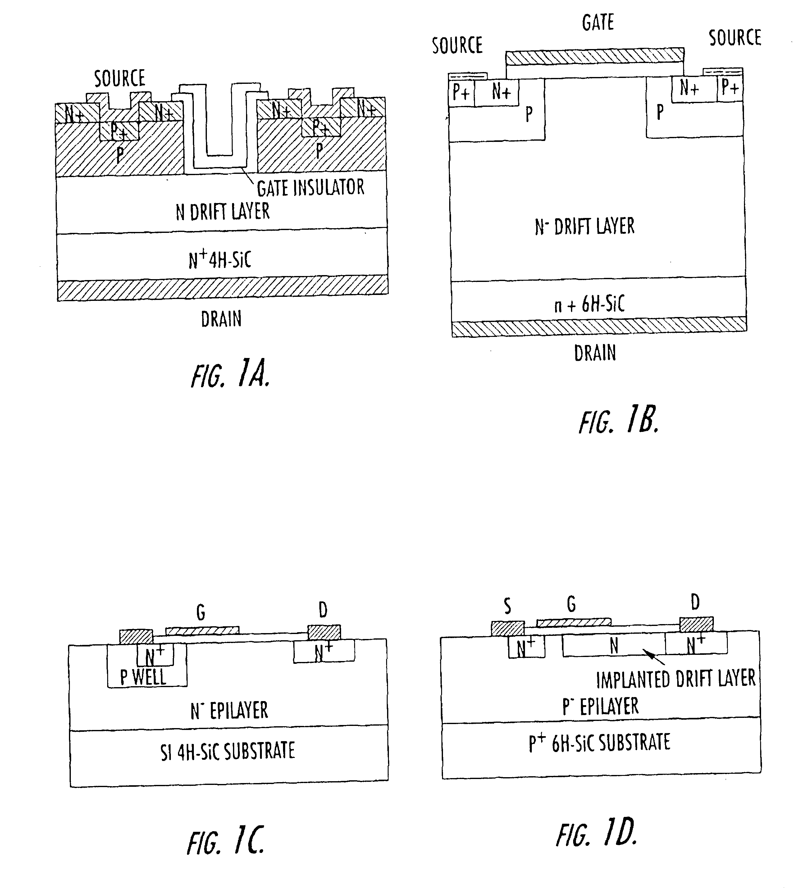
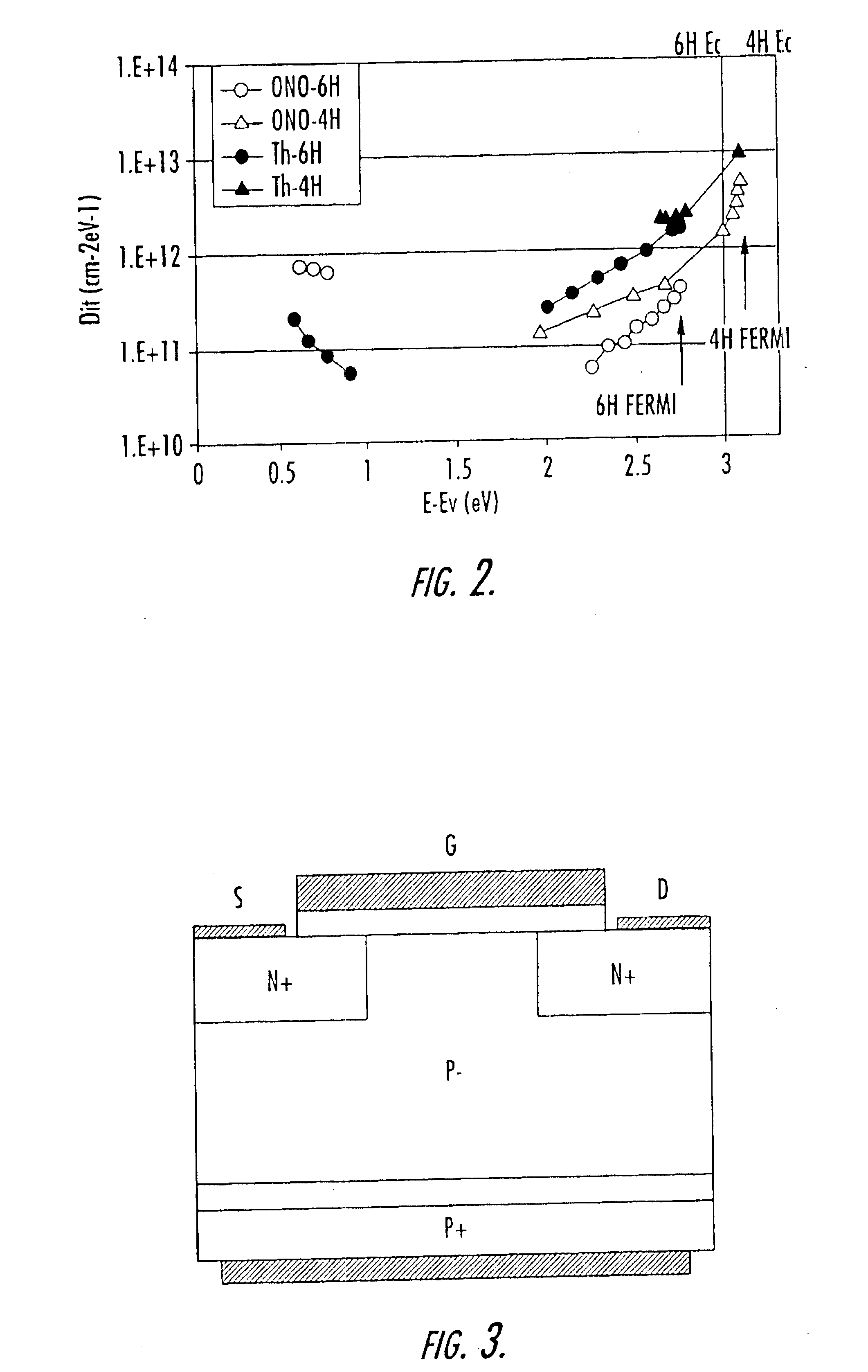
[0055]The present invention now will be described more fully hereinafter with reference to the accompanying drawings, in which preferred embodiments of the invention are shown. This invention may, however, be embodied in many different forms and should not be construed as limited to the embodiments set forth herein; rather, these embodiments are provided so that this disclosure will be thorough and complete, and will fully convey the scope of the invention to those skilled in the art. As illustrated in the Figures, the sizes of layers or regions are exaggerated for illustrative purposes and, thus, are provided to illustrate the general structures of the present invention. Like numbers refer to like elements throughout. It will be understood that when an element such as a layer, region or substrate is referred to as being “on” another element, it can be directly on the other element or intervening elements may also be present. In contrast, when an element is referred to as being “dir...


PUM

PropertyMeasurementUnit
carrier concentrationaaaaaaaaaa
conduction band energyaaaaaaaaaa
depthaaaaaaaaaa

Abstract

Silicon carbide metal-oxide semiconductor field effect transistors (MOSFETs) and methods of fabricating silicon carbide MOSFETs are provided. The silicon carbide MOSFETs have an n-type silicon carbide drift layer, spaced apart p-type silicon carbide regions in the n-type silicon carbide drift layer and having n-type silicon carbide regions therein, and a nitrided oxide layer. The MOSFETs also have n-type shorting channels extending from respective ones of the n-type silicon carbide regions through the p-type silicon carbide regions to the n-type silicon carbide drift layer. In further embodiments, silicon carbide MOSFETs and methods of fabricating silicon carbide MOSFETs are provided that include a region that is configured to self-deplete the source region, between the n-type silicon carbide regions and the drift layer, adjacent the oxide layer, upon application of a zero gate bias.

Description

RELATED APPLICATIONS[0001]The present application claims priority from U.S. Provisional Application Ser. No. 60 / 237,822, entitled “Method of Improving an Interface Between a Silicon Carbide Layer and an Oxide Layer,” U.S. Provisional Application Ser. No. 60 / 237,426 entitled “SiC Power MOSFET and Method of Fabrication” which were filed Oct. 3, 2000, U.S. Provisional Application Ser. No. 60 / 294,307 entitled “Method of N2O Growth of an oxide layer on a Silicon Carbide Layer” filed May 30, 2001, and U.S. patent application Ser. No. 09 / 834,283, entitled “Method of N2O Annealing an oxide layer on a Silicon Carbide Layer” filed Apr. 12, 2001, the disclosures of which are incorporated by reference as if set forth fully herein.STATEMENT OF GOVERNMENT INTEREST[0002]The present invention was made, at least in part, with support from United States Office of Naval Research contract number N00014-99-C-0377. The government may have certain rights in this invention.FIELD OF THE INVENTION[0003]The p...

Claims


Application Information

Patent Timeline
Patent Type & Authority Patents(United States)
IPC IPC(8): H01L29/66H01L21/02H01L29/10H01L29/78H01L21/04H01L29/02H01L29/24H01L21/336H01L29/12
CPCH01L21/049H01L29/1095H01L29/7828H01L29/7802H01L29/66068H01L29/1608H01L29/7838H01L29/78
Inventor RYU, SEI-HYUNGAGARWAL, ANANTDAS, MRINAL KANTILIPKIN, LORI A.PALMOUR, JOHN W.SINGH, RANBIR
Owner CREE INC
Why Eureka
Try Eureka