

Semiconductor device and method for manufacturing the same
a semiconductor and circuit technology, applied in semiconductor devices, capacitors, instruments, etc., can solve the problems of difficult to form a cmos logic section and a dram section together difficult to provide, and on the same chip, etc., to achieve sufficient signal holding characteristic, reduce power consumption, and increase processing speed
- Summary
- Abstract
- Description
- Claims
- Application Information
AI Technical Summary
Benefits of technology
Problems solved by technology
Method used
Image

Examples
first embodiment
[0068]A semiconductor device according to the first embodiment of the present invention will now be described with reference to the drawings.
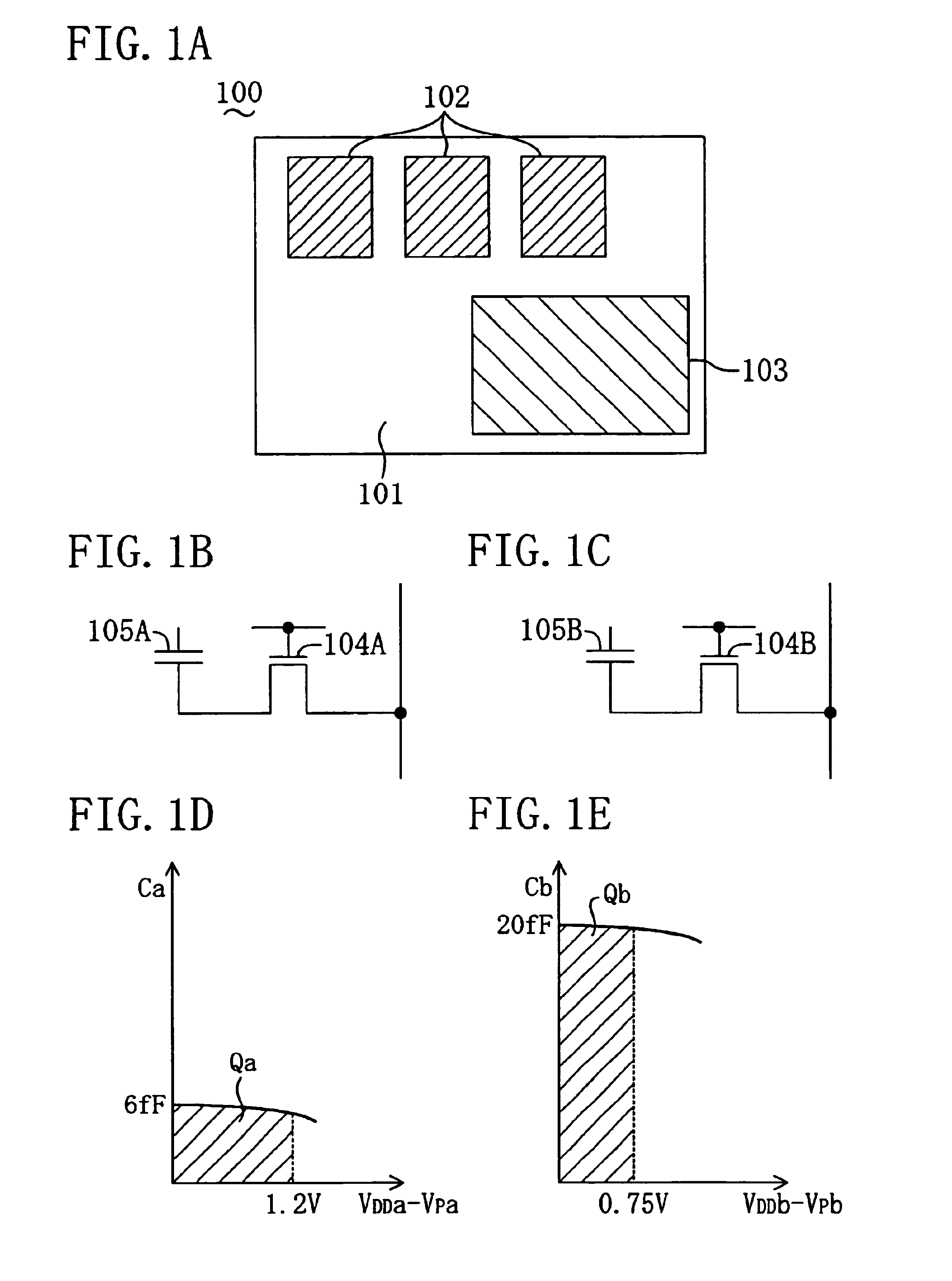
[0069]FIG. 1A is a plan view illustrating a general configuration of the semiconductor device according to the first embodiment of the present invention.
[0070]As illustrated in FIG. 1A, a CMOS logic section 101 is formed on a chip 100, and a first DRAM section 102 and a second DRAM section 103 are formed on the same chip 100. The first DRAM section 102 is intended to provide temporary storage of data being processed at a high speed, i.e., to store a charge that is moved at a high speed. In contrast, the second DRAM section 103 is intended to hold a signal written thereto sufficiently long.
[0071]A feature of the present embodiment is that the capacitances of the memory cells of the first DRAM section 102 and the second DRAM section 103 are individually set for their respective applications.
[0072]FIG. 1B and FIG. 1C are equivalent circuit diagram...
second embodiment
[0080]A semiconductor device according to the second embodiment and a method for manufacturing the same will now be described with reference to the drawings. Also in the present embodiment, the general configuration of the semiconductor device is as shown in the plan view of FIG. 1A.
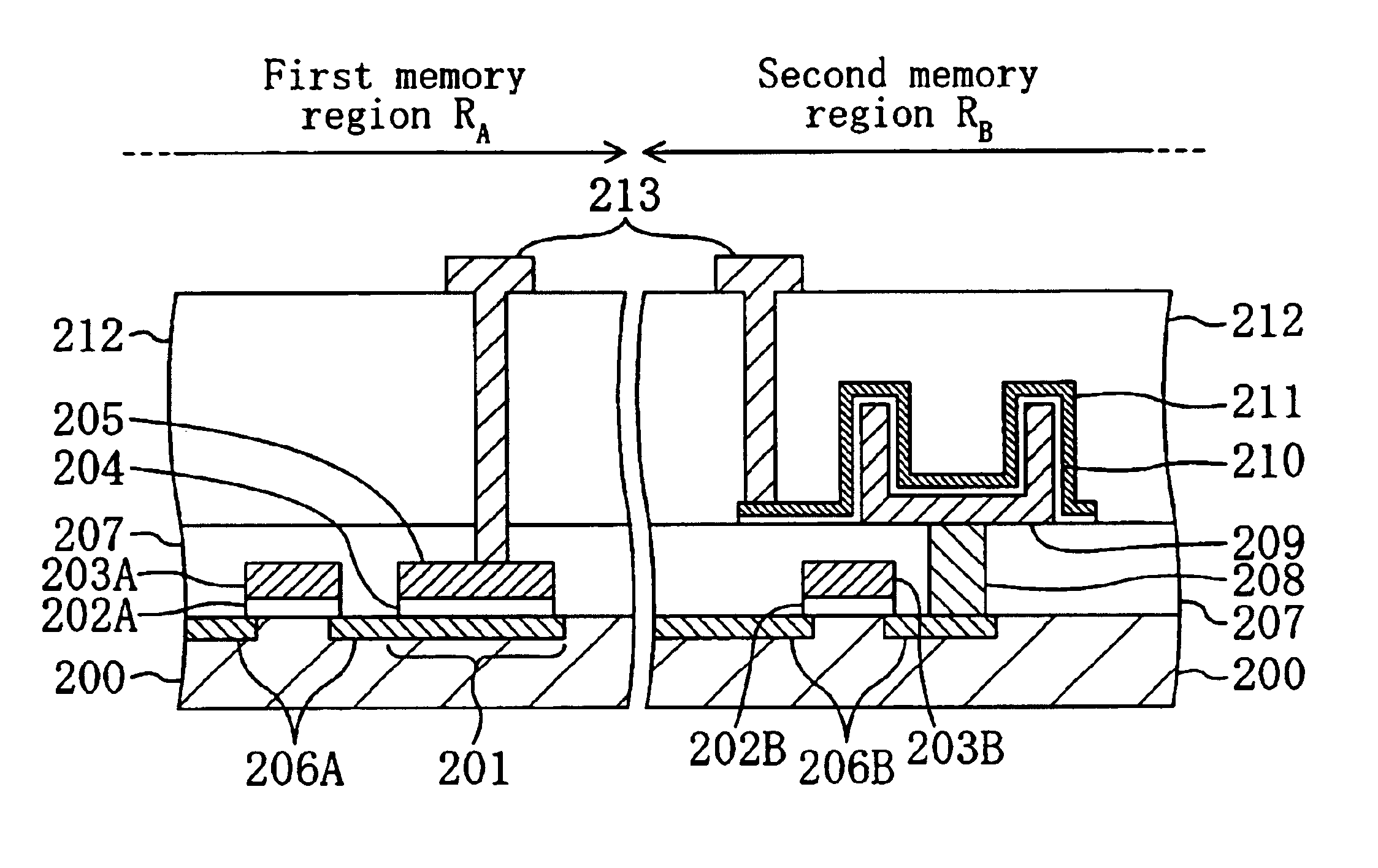
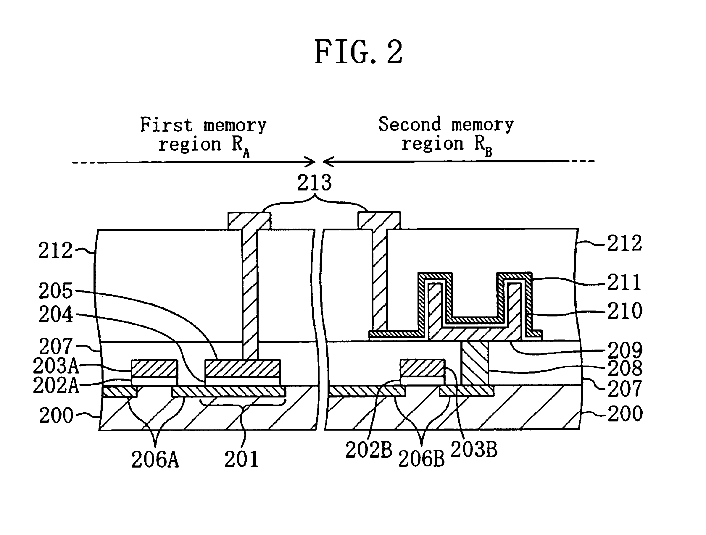
[0081]FIG. 2 is a cross-sectional view illustrating the semiconductor device according to the second embodiment. More specifically, FIG. 2 shows memory cells of the first DRAM section 102 and the second DRAM section 103 formed on the chip 100 illustrated in FIG. 1A. Note that the two regions where the first DRAM section 102 and the second DRAM section 103 are formed are referred to as “first memory region RA” and “second memory region RB”, respectively.
[0082]As illustrated in FIG. 2, a first gate electrode 203A is formed on a semiconductor substrate 200 in the first memory region RA with a first gate insulating film 202A interposed between the semiconductor substrate 200 and the first gate electrode 203A...
third embodiment
[0103]A semiconductor device according to the third embodiment and a method for manufacturing the same will now be described with reference to the drawings. Also in the present embodiment, the general configuration of the semiconductor device is as shown in the plan view of FIG. 1A.
[0104]FIG. 5 is a cross-sectional view illustrating the semiconductor device according to the third embodiment. More specifically, FIG. 5 shows memory cells of the first DRAM section 102 and the second DRAM section 103 formed on the chip 100 illustrated in FIG. 1A. Note that the two regions where the first DRAM section 102 and the second DRAM section 103 are formed are referred to as “first memory region RA” and “second memory region RB”, respectively.
[0105]As illustrated in FIG. 5, a first gate electrode 302A is formed on a semiconductor substrate 300 in the first memory region RA with a first gate insulating film 301A interposed between the semiconductor substrate 300 and the first gate electrode 302A. ...
PUM
 Abstract
Description
Claims
Application Information