Structure and method for latchup suppression utilizing trench and masked sub-collector implantation

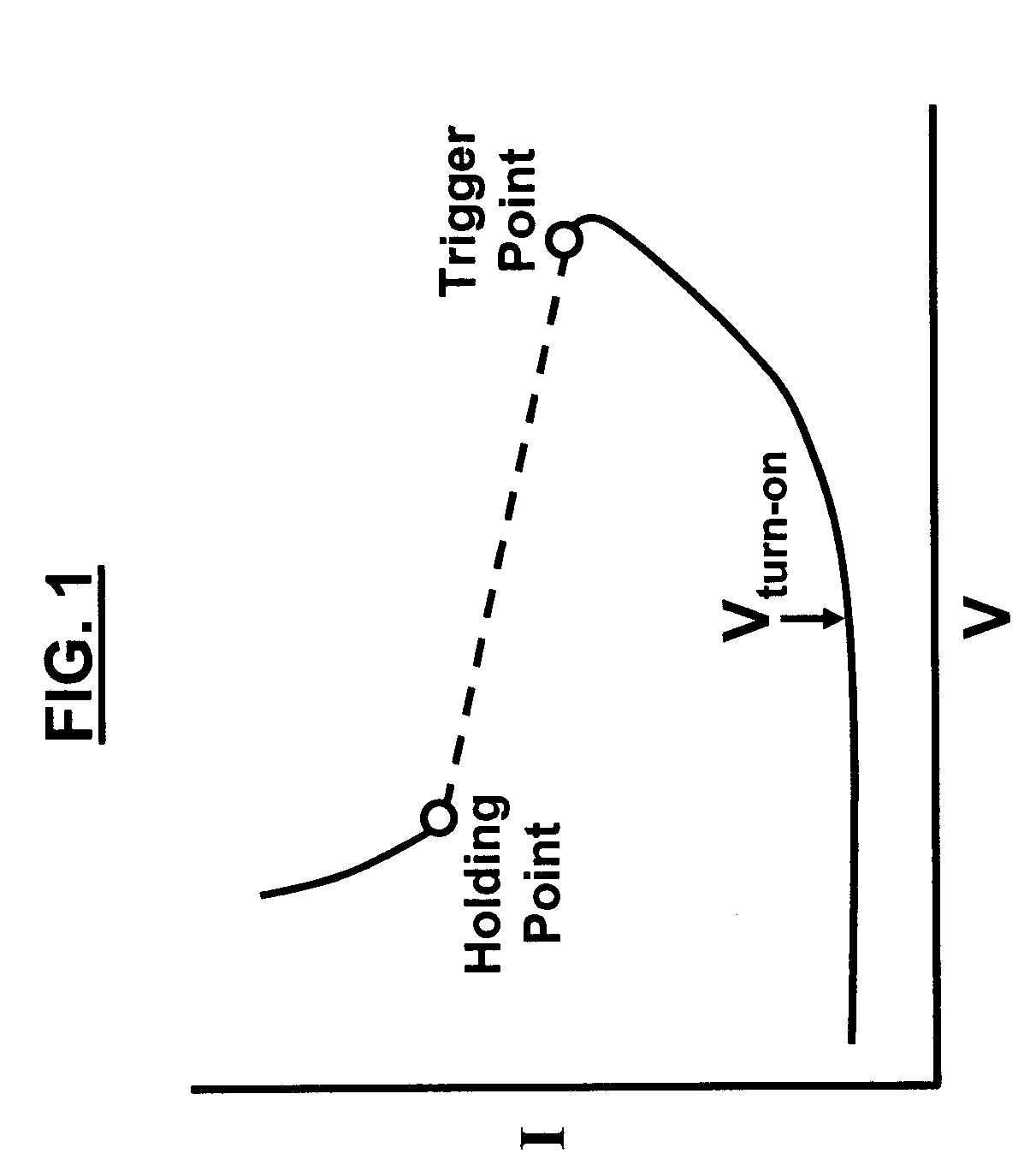
a sub-collector and trench technology, applied in the direction of semiconductor devices, electrical equipment, transistors, etc., can solve the problems of noise injection and latchup conditions, increased likelihood of latchup, injection of substrate, etc., to improve latchup robustness, improve latchup robustness, and improve the effect of vturnon

Inactive Publication Date: 2005-10-18
GLOBALFOUNDRIES INC
View PDF24 Cites 63 Cited by
  • Summary
  • Abstract
  • Description
  • Claims
  • Application Information

AI Technical Summary

Benefits of technology

[0020]The embodiments of the invention improve the latchup robustness in CMOS devices. A trench isolation region or deep trench structure and a highly doped region, such as a n-type sub-collector, are formed in proximity to a CMOS device. A portion of the trench sidewall on the device side of the trench is in contact with the high dopant region. The high dopant region is formed below the CMOS device area and can be configured as a continuous or masked dopant region. The trench and high dopant region prevent carriers from going under the trench, thus Vturnon is increased and the CMOS device's latchup robustness is improved.

Problems solved by technology

In CMOS I / O circuitry, undershoot and overshoot can lead to injection in the substrate.
Simultaneous switching of circuitry where overshoot or undershoot injection occurs, leads to injection into the substrate which leads to both noise injection and latchup conditions.
Moreover, ESD elements connected to the input pad can also lead to latchup.
ESD circuits can also contribute to noise injection into the substrate and latchup.
Unfortunately, this implementation can lead to latchup.
In an ASIC gate array environment, it has been observed that as a negative pulse is injected into an input pad, ESD current discharge to the substrate flows outside of the I / O cell region, leading to “turn-on” of the adjacent gate array regions connected to the VSS and VDD rails, which often results in an increased likelihood of latchup, and leads to the failure of the latchup specification.
With the scaling of the shallow trench isolation (STI) for aspect ratio, the vulnerability of CMOS technology to latchup has increased.
Furthermore, vertical scaling of the wells, and lower n-well and p-well implant doses also has increased the lateral parasitic bipolar current gains, leading to lower latchup robustness.
Terrestrial emissions from radioactive events, such as alpha particles, and other radioactive decay emissions can also lead to latchup in semiconductors.
Latchup can lead to failure of space applications triggered by cosmic rays, heavy ions, and proton and neutron events.

Method used


Image

  • Structure and method for latchup suppression utilizing trench and masked sub-collector implantation
  • Structure and method for latchup suppression utilizing trench and masked sub-collector implantation
  • Structure and method for latchup suppression utilizing trench and masked sub-collector implantation

Examples


Embodiment Construction

Embodiments of the Invention

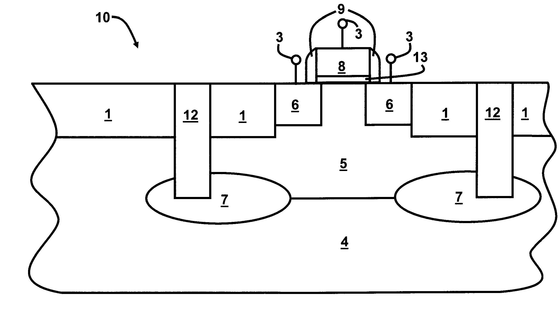
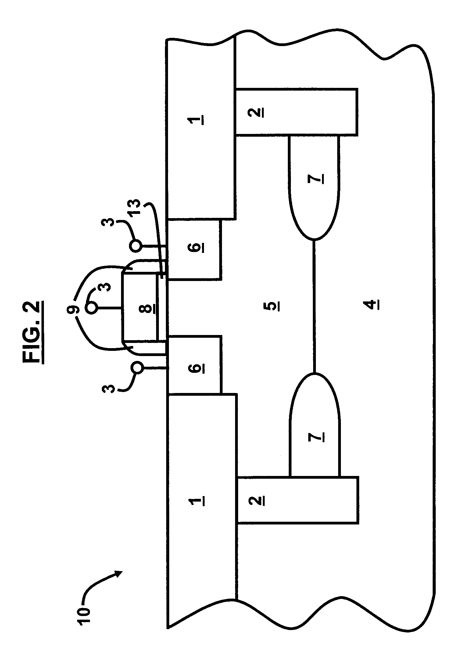
[0039]The embodiments of the invention and the various features and advantageous details thereof are explained more fully with reference to the non-limiting embodiments that are illustrated in the accompanying drawings and detailed in the following description. It should be noted that the features illustrated in the drawings are not necessarily drawn to scale. Descriptions of well-known components and processing techniques are omitted so as to not unnecessarily obscure the embodiments of the invention. The examples used herein are intended merely to facilitate an understanding of ways in which the embodiments of the invention may be practiced and to further enable those of skill in the art to practice the embodiments of the invention. Accordingly, the examples should not be construed as limiting the scope of the embodiments of the invention.

[0040]As mentioned, there remains a need for a structure and method that improves the latchup tolerance in base CMOS...


PUM


Abstract

A method and structure for an integrated circuit comprising a substrate of a first polarity; a trench structure in the substrate; a well region of a second polarity abutting the trench structure; and a heavily doped region of the second polarity abutting the trench structure, wherein the heavily doped region is adapted to suppress latch-up in the integrated circuit, wherein the heavily doped region comprises a sub-collector region, and wherein the trench structure comprises a deep trench structure or a trench isolation structure. The integrated circuit further comprises a p+ anode in the well region and a n+ cathode in the well region, wherein the integrated circuit is configured as a latchup robust p-n diode. In another embodiment, the integrated circuit further comprises a p+ anode in the well region; a n+ cathode in the well region; and a gate structure over the p+ anode and n+ cathode.

Description

BACKGROUND OF THE INVENTION[0001]1. Field of the Invention[0002]The embodiments of the invention generally relate to integrated circuits, and more particularly to providing latchup suppression in integrated circuits.[0003]2. Description of the Related Art[0004]As electronic components continue to become smaller along with the internal structures in integrated circuits, it is getting easier to either completely destroy or otherwise impair the electronic components from latchup. Latchup occurs when a pnpn structure transitions from a low current high voltage state to a high current low voltage state through a negative resistance region (i.e., forming an S-Type I-V (current / voltage) characteristic).[0005]Latchup is typically understood as occurring within a pnpn structure, or silicon controlled rectifier (SCR) structure. It is possible for these pnpn structures to be intentionally designed, or even unintentionally formed between structures. Hence, latchup conditions can occur within pe...

Claims


Application Information

Patent Timeline
Patent Type & Authority Patents(United States)
IPC IPC(8): H01L29/66H01L29/76H01L31/062H01L31/06H01L29/94H01L31/101H01L31/113H01L31/115H01L31/119H01L21/762H01L21/8238H01L27/092H01L29/78
CPCH01L21/76237H01L21/823878H01L27/0921H01L29/78
Inventor VOLDMAN, STEVEN H.WATSON, ANNE E.
Owner GLOBALFOUNDRIES INC
Why Eureka
Try Eureka