Semiconductor memory device and control method thereof
a memory device and semiconductor technology, applied in static storage, digital storage, instruments, etc., can solve the problems of no data access time being shortened, no data access at high speed being realized, and no time of refresh operation cycle being shortened, so as to shorten the refresh operation cycle and improve the data transfer rate. , the effect of speed
- Summary
- Abstract
- Description
- Claims
- Application Information
AI Technical Summary
Benefits of technology
Problems solved by technology
Method used
Image

Examples
first embodiment
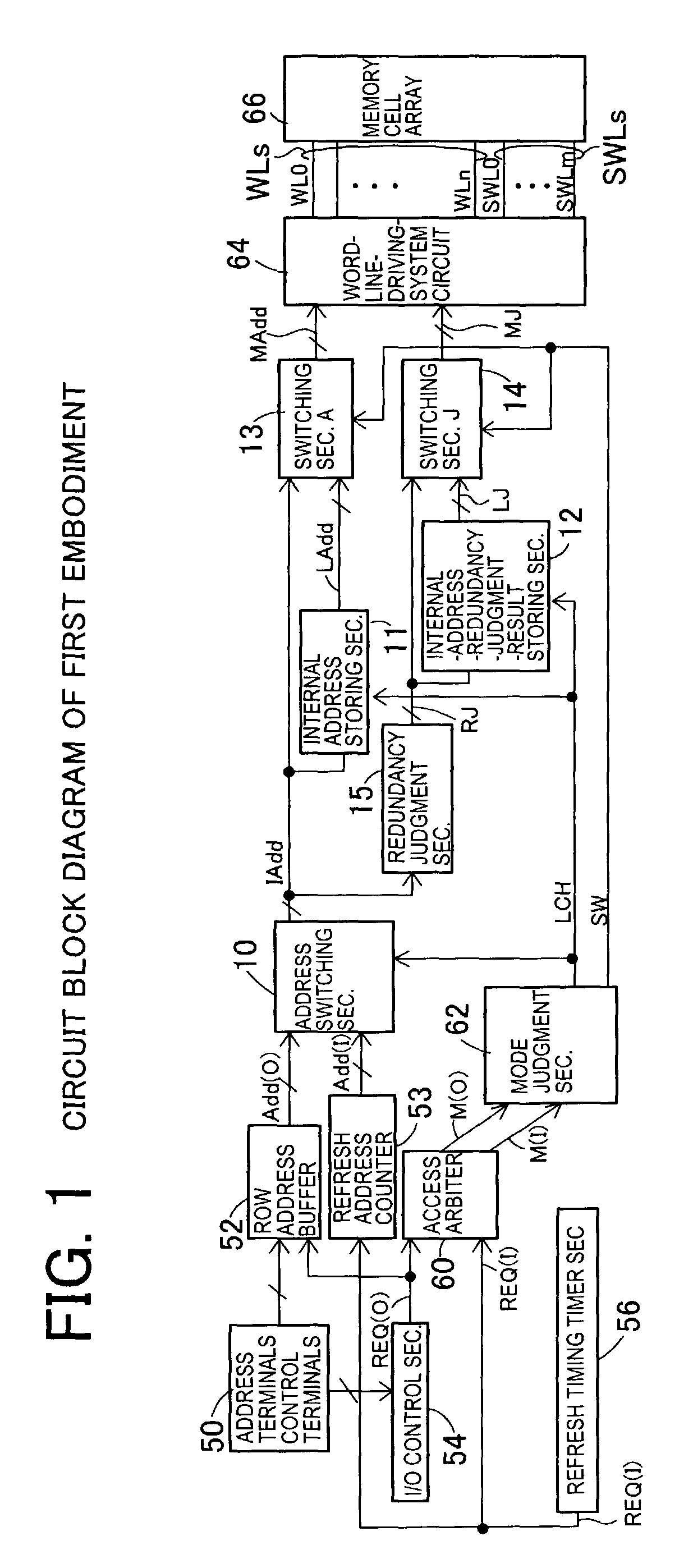
[0052]A first embodiment shown in FIG. 1 is a case in which the present invention is applied to the semiconductor memory device of an operation specification for mutually independently performing a built-in refresh operation and a data access operation from the exterior in timing of occasion demands. Since a refresh operation mode and a data access operation mode can be mutually independently operated, no external controller for the refresh operation is required, and interchangeability with an SRAM such as a pseudo-SRAM, etc. is set to be more perfect in the semiconductor memory device. FIG. 1 shows only a portion relative to a row address system.
[0053]Predetermined control terminals 50 are connected to an I / O control section 54, and output an external-access request signal REQ (O) in accordance with control signals inputted from the control terminals 50. The external-access request signal REQ(O) is transmitted to a row address buffer 52 together with address signals inputted from t...
second embodiment
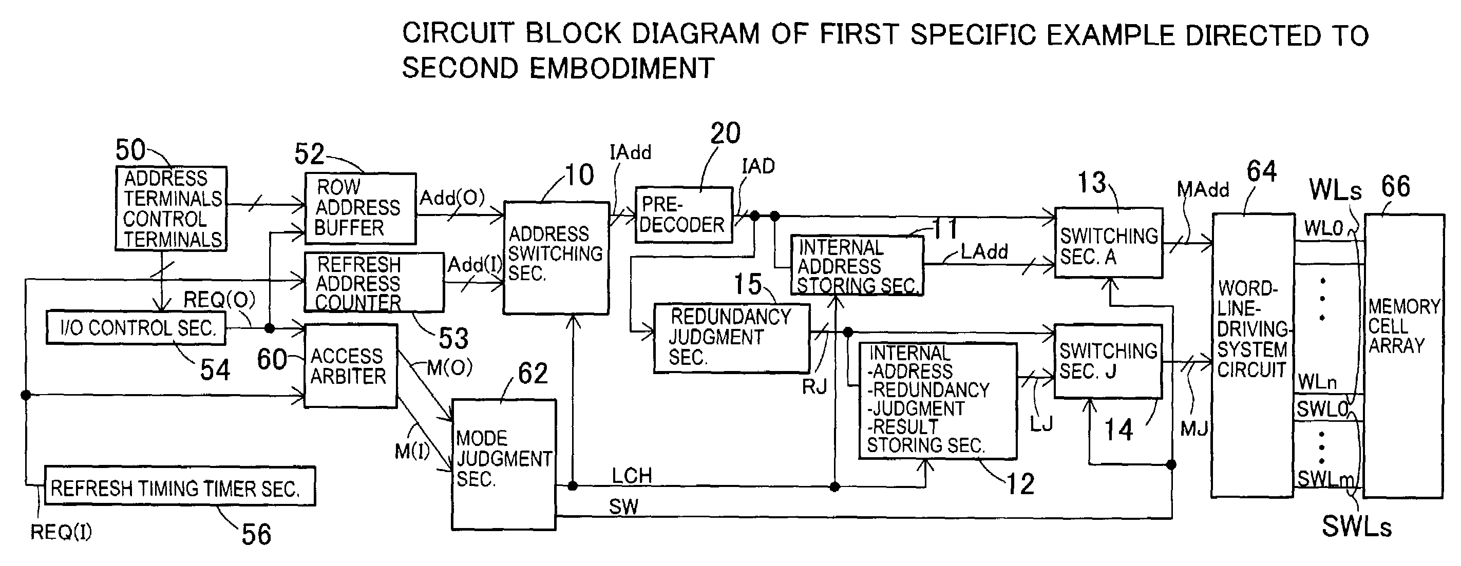
[0107]Similar to the case shown in FIG. 6, FIG. 10 shows a layout arrangement example when the semiconductor memory device of the first concrete example of the second embodiment is divided into four memory banks A to D. Main decoders MD0 to MD3 of the word-line-driving-system circuit 64 and word line drivers WD0 to WD3 are arranged in proximity to the memory cell array in each of the banks A to D. The row address buffer 52, the refresh address counter 53 and the address switching section 10 are arranged in the entire chip along the chip long side direction near the center of a short side of the chip. Therefore, in the case of long distance wiring, parasitic resistance RLD and parasitic capacity CLD are increased. Further, each of the main decoders MD0 to MD3 for inputting address information thereto from the pre-decoder 20 is constructed by a logic gate of many inputs in accordance with the address bit width, and has large input capacity. Accordingly, it is necessary to devise the c...
third embodiment
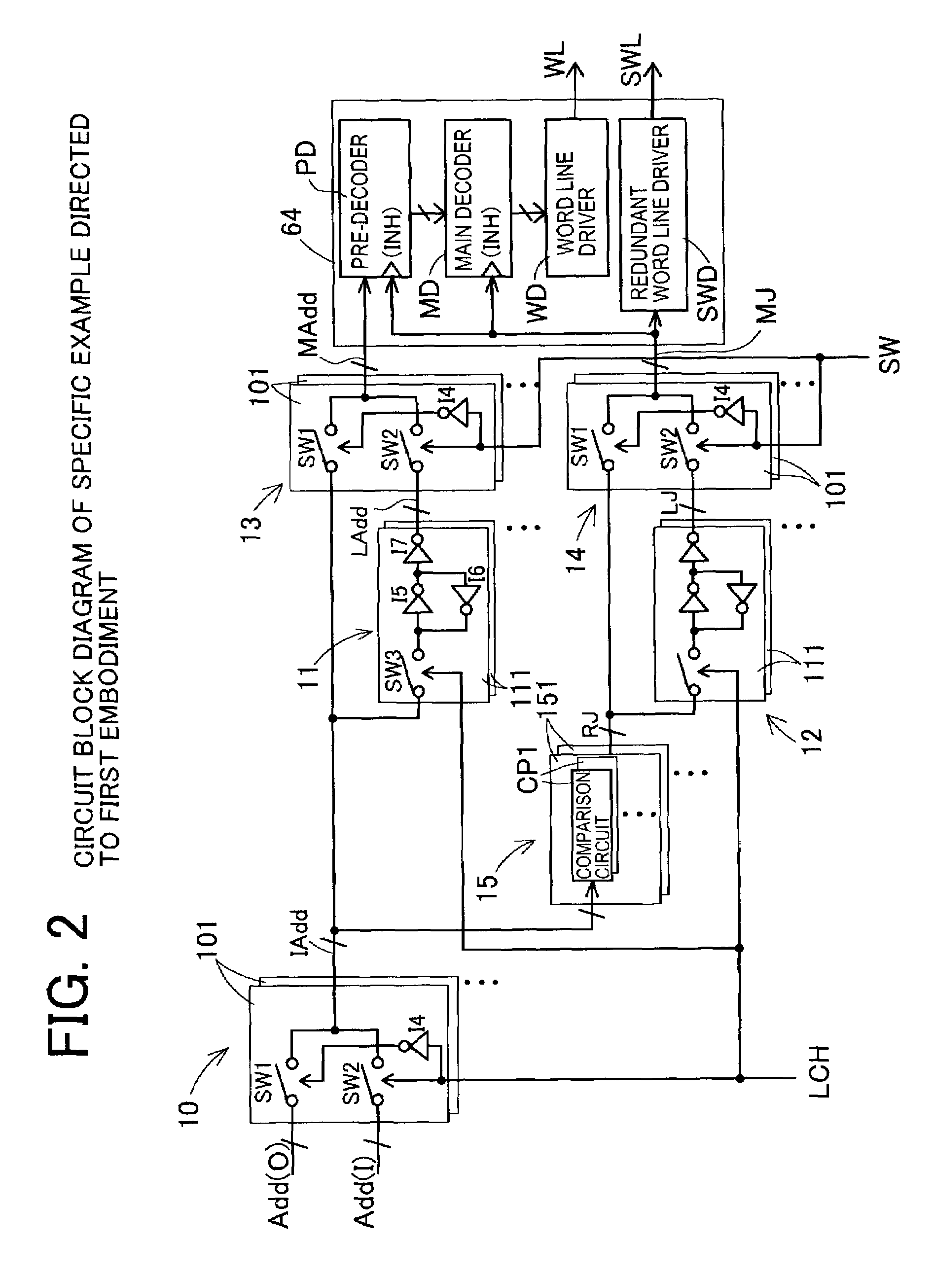
[0117]FIG. 13 shows operational waveforms of the control signals LCH(O), LCH(I), SW with respect to the mode signals M(O), M(I) in the operation of the semiconductor memory device in the In FIG. 13, the mode signals M(O), M(I) are inputted as pulse signals at high levels.
[0118]When the pulse signal of the refresh operation mode signal M(I) is inputted, the control signal SW is changed to the high level, and each switch section SW2 of each of the switching sections 13, 14 is set to a turning-on state. The stored refresh address Add(I) and redundancy judgment result RJ(I) are fetched to the word-line-driving-system circuit 64 from the stored address bus LAdd and the stored-redundancy-judgment-result bus LJ. A refresh operation activation signal RFACT is simultaneously changed to the high level by an unillustrated control circuit, and the refresh operation is started. When the refresh operation activation signal RFACT is then changed to the low level and the refresh operation is termi...
PUM
 Abstract
Description
Claims
Application Information
 - R&D
- Intellectual Property
- Life Sciences
- Materials
- Tech Scout
- Unparalleled Data Quality
- Higher Quality Content
- 60% Fewer Hallucinations
Browse by: Latest US Patents, China's latest patents, Technical Efficacy Thesaurus, Application Domain, Technology Topic, Popular Technical Reports.
© 2025 PatSnap. All rights reserved.Legal|Privacy policy|Modern Slavery Act Transparency Statement|Sitemap|About US| Contact US: help@patsnap.com