Acoustic detection of mechanically induced circuit damage

a technology of induced circuit damage and acoustic detection, which is applied in the testing/measurement of individual semiconductor devices, semiconductor/solid-state devices, instruments, etc., can solve problems such as scratching from manufacturing or handling equipment, defects of ic patterns on silicon wafers, and process of semiconductors under non-typical environmental conditions

Inactive Publication Date: 2005-10-25
POLARIS INNOVATIONS LTD
View PDF7 Cites 7 Cited by
  • Summary
  • Abstract
  • Description
  • Claims
  • Application Information

AI Technical Summary

Benefits of technology

[0011]According to an aspect of the present invention, there is provided a system initialization process for a normal production of an integrated circuit (IC) pattern of a wafer, including: acoustically auditing a semiconductor processing equipment to select mechanical components to be monitored; mounting one or more acoustic transducers and a recording device on the mechanical components selected for monitoring; monitoring each selected mechanical component only at predetermined manufacturing stages when there is a risk of the wafer from being damaged; recording output signals of the selected mechanical components when operating during the predetermined manufacturing stages; setting-up the mechanical components to make unwanted contact with a surface of the wafer; recording acoustic emission training set signals for pattern recognition of the output signals of the selected mechanical components when there is unwanted contact; adjusting back the selected mechanical components so that the mechanical components do not make unwanted contact with the surface of the wafer; recording the output signals generated by the selected mechanical components at the normal production as the sound signals; and beginning the normal production of the IC pattern and monitoring the output signals from the selected mechanical components for unwanted contact.

Problems solved by technology

Further, semiconductor processes take place under non-typical environmental conditions of temperature, pressure, atmospheric gaseous and liquid composition, and electromagnetic field intensity that are hostile to human life.
If a robot ceases to operate or if a mechanical component of the semiconductor processing equipment is misaligned or malfunctioning, defects of the IC pattern on the silicon wafer may occur.
Such defects may include scratching from the manufacturing or handling equipment coming into contact with the wafer or particles dispersed throughout the wafer from a manufacturing environment.
However, current ex-situ control of defect monitoring processes employ visual inspection and / or optical testing of the silicon wafers to detect scratching.
Thus, if scratching occurs during first few manufacturing operations of the manufacturing of the IC pattern on the wafer, the wafer is not inspected for defects until after a number of manufacturing operations have occurred or after the manufacturing process is complete, which could be after many hours or days.
Due to batch processing considerations and other factors introducing delay between the manufacturing and analysis of the silicon wafers for scratching, a large number of the silicon wafers may become scratched by one of the mechanical components of the semiconductor processing equipment before such scratching is detected.
Further, when the defective mechanical component is identified, production is stopped and corrective maintenance is performed on the equipment, thereby a significant time delay exists between occurrence of the scratching and detection of the defective mechanical component.
Thus, typically a minimum of 25 wafers—and often as many as 400 wafers or more—may be damaged or destroyed before a detection of the problem.

Method used


Image

  • Acoustic detection of mechanically induced circuit damage
  • Acoustic detection of mechanically induced circuit damage
  • Acoustic detection of mechanically induced circuit damage

Examples


Embodiment Construction

[0022]Reference will now be made in detail to the aspects of the present invention, examples of which are illustrated in the accompanying drawings, wherein like reference numerals refer to like elements throughout. The aspects are described below in order to explain the present invention by referring to the figures.

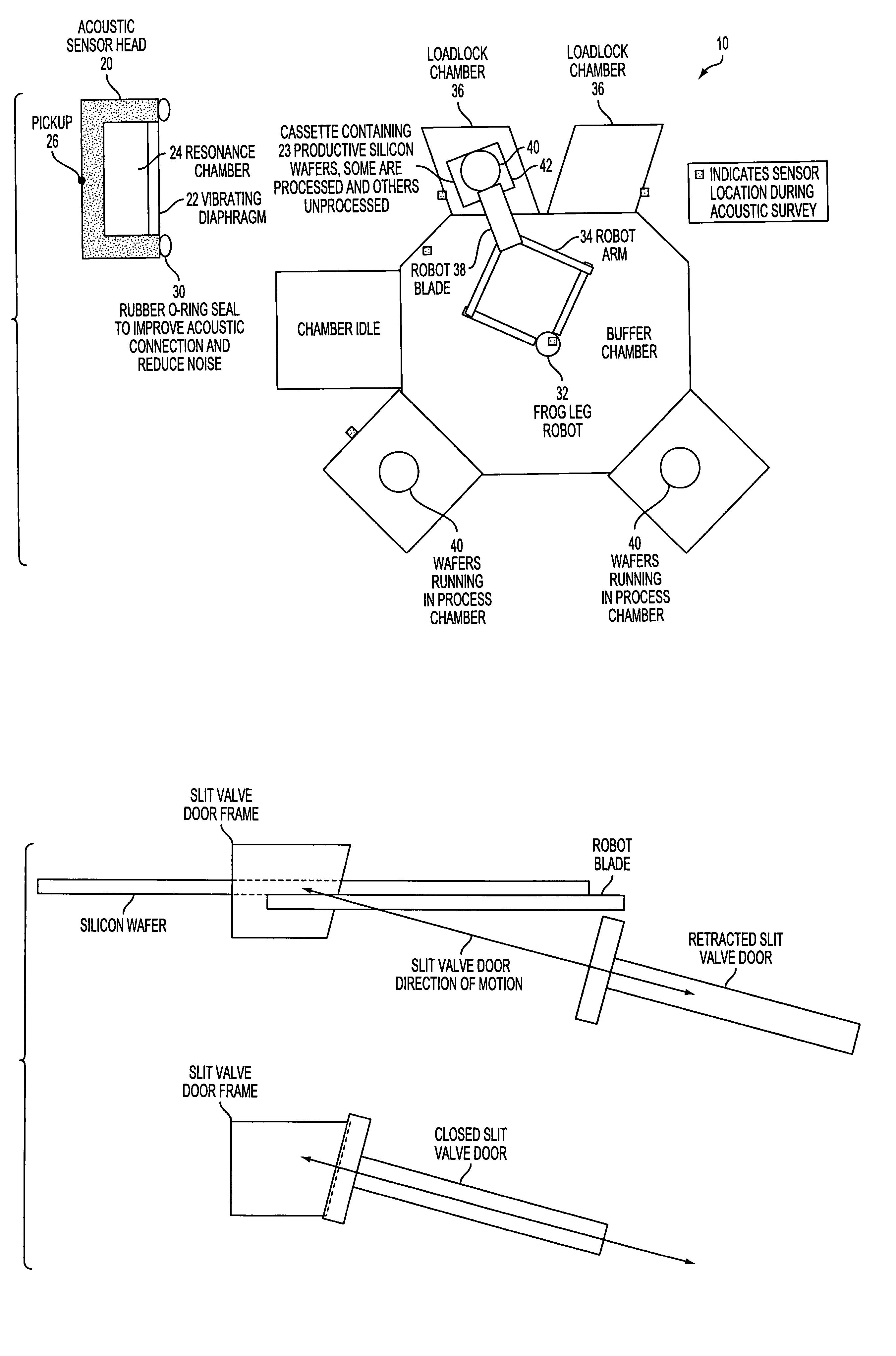
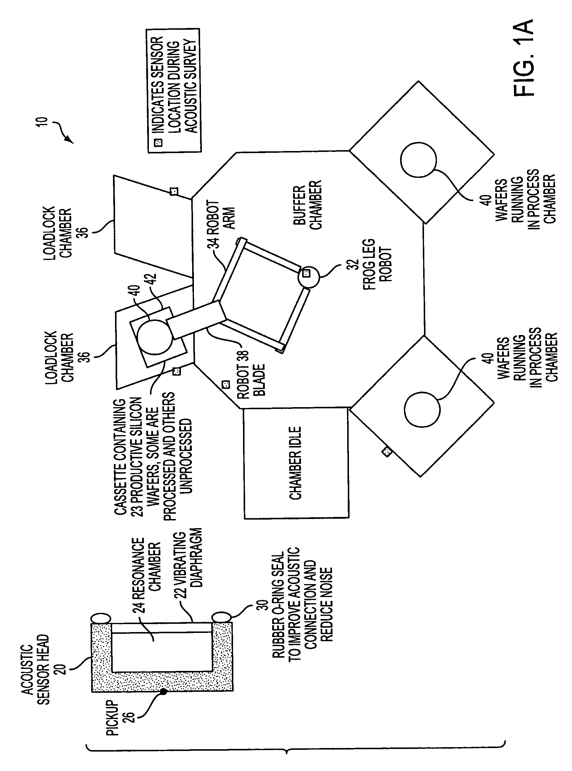
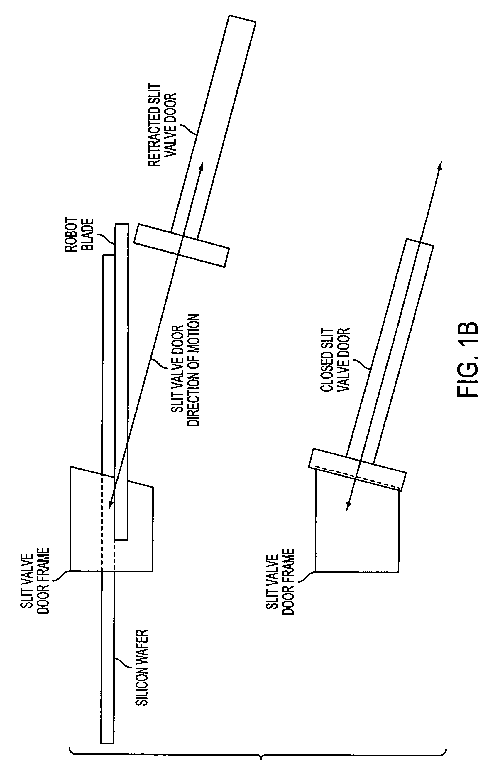
[0023]FIG. 1A is a diagram illustrating a system architecture using acoustic emission transducers 20 to detect an in-situ failure of mechanical components of a semiconductor processing equipment 10 to significantly reduce damage done to circuit patterns on semiconductor products and limit manufacturing costs and limit significant yield loss, in accordance with an aspect of the present invention. In-situ is defined as inspecting in real-time the semiconductor produce during the manufacturing / handling processing of the semiconductor product, that is, during a time where the manufacturing / handling processing of the semiconductor product occurs.

[0024]According to an aspect of...


PUM

PropertyMeasurementUnit
processingaaaaaaaaaa
currentaaaaaaaaaa
conductingaaaaaaaaaa

Abstract

An apparatus and method thereof includes at least one acoustic transducer for receiving acoustic emissions produced during a semiconductor fabrication process. The acoustic transducer is mounted to various mechanical components of a semiconductor processing equipment in a manner so that the acoustic transducer receives acoustic emissions produced during the fabrication process. The received acoustic emissions are analyzed in in-situ to identify and determine surface characteristics of the wafer.

Description

BACKGROUND OF THE INVENTION[0001]1. Field of the Invention[0002]The present invention relates to an acoustic detection apparatus and method to acoustically detect induced circuit damage caused by semiconductor manufacturing equipment handling systems.[0003]2. Description of the Related Art[0004]Fabricating an integrated circuit (IC) typically includes sequentially depositing conducting, semiconducting and / or insulating layers on a silicon wafer. One fabrication step includes depositing a metal layer over previous layers and planarizing the metal layer. For example, trenches or holes in an insulating layer may be filled with a conducting metal. After a chemical mechanical polishing (CMP) planarization, portions of the conductive metal remaining between the raised patterns of an insulating layer may form, for example, vias, plugs and / or lines.[0005]Further, semiconductor processes take place under non-typical environmental conditions of temperature, pressure, atmospheric gaseous and l...

Claims


Application Information

Patent Timeline
Patent Type & Authority Patents(United States)
IPC IPC(8): H01L21/00
CPCG01N29/14H01L21/67259G01N2291/2697Y02P80/30
Inventor GILGUNN, PETER
Owner POLARIS INNOVATIONS LTD
Why Eureka
Try Eureka