Multiprobe detection system for chemical-mechanical planarization tool

Inactive Publication Date: 2005-11-01
NOVELLUS SYSTEMS
View PDF6 Cites 20 Cited by
  • Summary
  • Abstract
  • Description
  • Claims
  • Application Information

AI Technical Summary

Benefits of technology

[0019]Orbital CMP tools, due to their generally small orbital radius in comparison to the size of the wafer, are advantageous in that they allow a majority of the probes to continuously remain under the wafer during the planarization process. In addition, due to the typical motions in an orbital CMP tool, each probe tends to take all its measurements within a single concentric band on the front surface of the wafer simplifying the analysis. The bands may be allowed to overlap to insure the entire front surface of the wafer is being monitored and to enable health monitoring of the various probes. The measurements

Problems solved by technology

Other types of CMP tools may also be used, but they will generally receive data for a

Method used


Image

  • Multiprobe detection system for chemical-mechanical planarization tool
  • Multiprobe detection system for chemical-mechanical planarization tool
  • Multiprobe detection system for chemical-mechanical planarization tool

Examples


Embodiment Construction

[0028]An improved polishing apparatus and method utilized in the polishing of semiconductor wafers and thin films formed thereon will now be described. In the following description, numerous specific details are set forth illustrating Applicant's best mode for practicing the present invention and enabling one of ordinary skill in the art to make and use the present invention. It will be known, however, to one skilled in the art that the present invention may be practiced without these specific details. In other instances, well-known machines and process steps have not been described in particular detail in order to avoid unnecessarily obscuring the present invention.

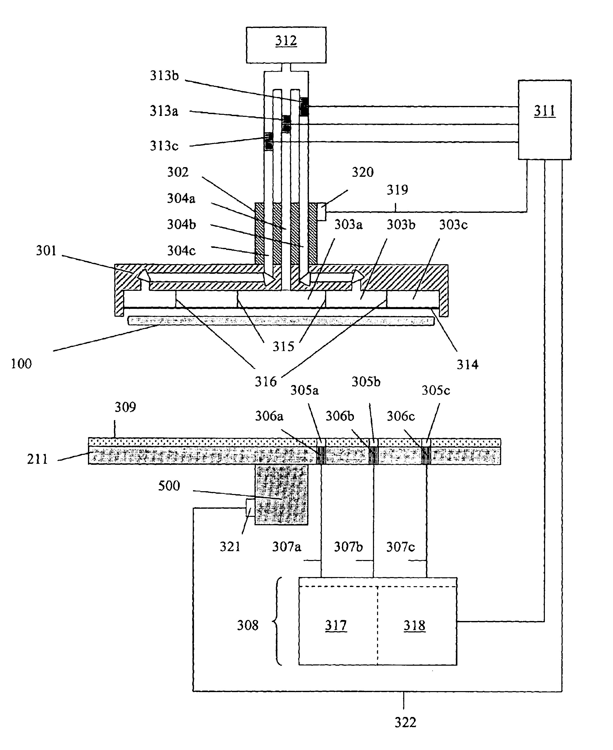
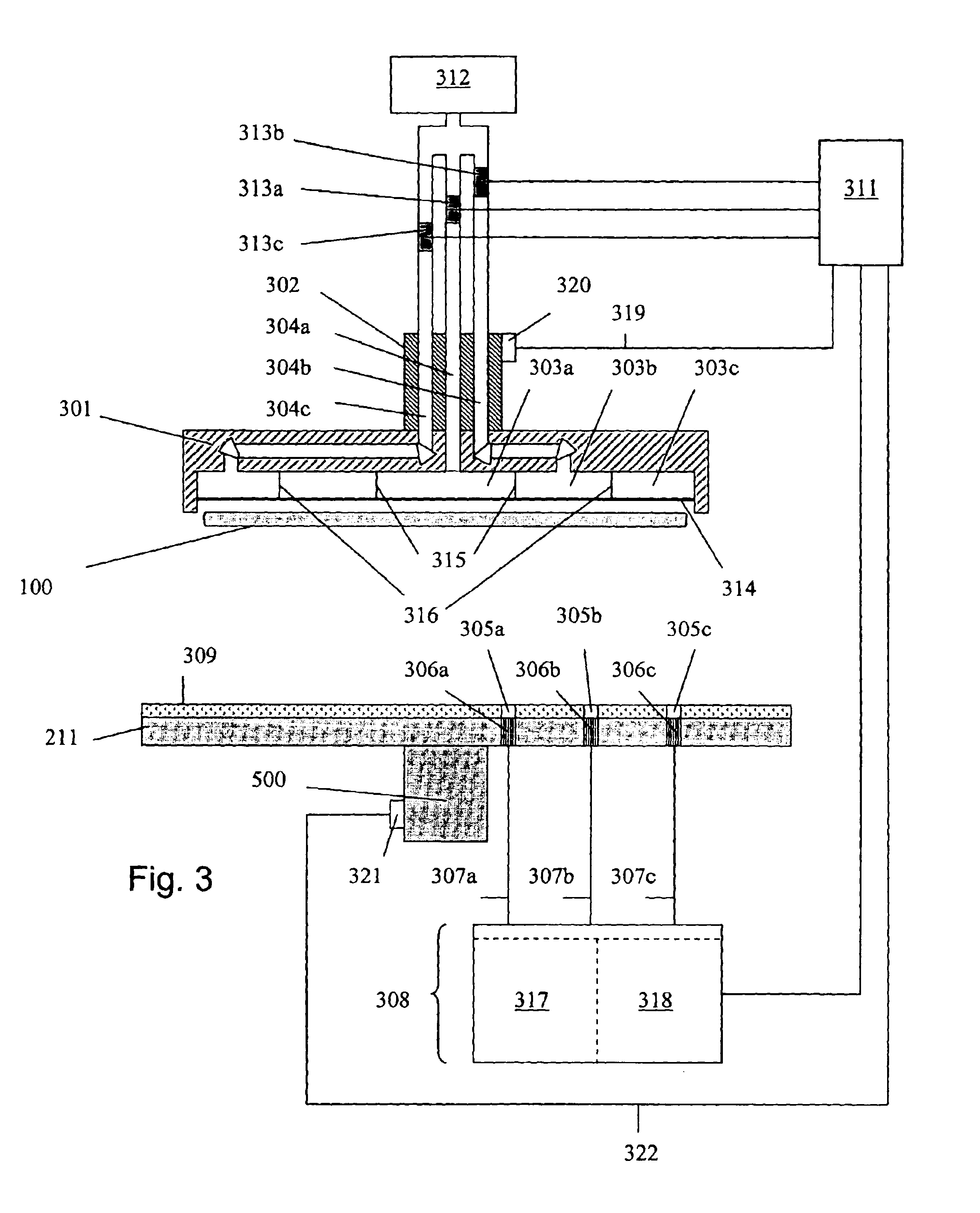
[0029]An apparatus for practicing the present invention will now be discussed with reference to FIG. 3. During a planarization process, a wafer 100 may be transported by a carrier 301 to a position adjacent and substantially parallel to a working surface or polishing pad 309. The front surface of the wafer 100 is pressed...


PUM

PropertyMeasurementUnit
Timeaaaaaaaaaa
Pressureaaaaaaaaaa
Areaaaaaaaaaaa

Abstract

The invention is a method and apparatus for planarizing a wafer. Discrete measurements are taken across the surface of the wafer at a desired spatial density. The measurements may be generated using a flash lamp to reflect a light signal off the surface of the wafer with a spectrometer analyzing the reflected light. A plurality of probes may be used at different locations to shorten the time necessary for taking measurements across the full front surface of the wafer and for allowing a plurality of areas to be sampled substantially simultaneously. A control system receives the measurements and their corresponding locations. The control system is then able to analyze the data looking for areas or bands on the front surface of the wafer that need an increase or decrease in material removal rate. The control system is then able to adjust one or more planarization parameters to improve the process for the current wafer or for future wafers.

Description

CROSS REFERENCE TO RELATED APPLICATIONS[0001]This is a divisional of patent application Ser. No. 09 / 690,521 filed on Oct. 17, 2000 now U.S. Pat. No. 6,805,613.TECHNICAL FIELD[0002]The present invention relates generally to semiconductor manufacturing and more specifically to monitoring in situ a planarization process of a wafer with a plurality of probes and feeding back the information to improve the planarization process.BACKGROUND OF THE INVENTION[0003]A flat disk or “wafer” of single crystal silicon is the basic substrate material in the semiconductor industry for the manufacture of integrated circuits. Semiconductor wafers are typically created by growing an elongated cylinder or boule of single crystal silicon and then slicing individual wafers from the cylinder. The slicing causes both faces of the wafer to be extremely rough. The front face of the wafer on which integrated circuitry is to be constructed must be extremely flat in order to facilitate reliable semiconductor jun...

Claims


Application Information

Patent Timeline
IPC IPC(8): B24B49/00B24B37/04B24B49/14B24B49/12B24B49/10H01L21/00B24B37/013B24B37/10B24B37/30
CPCB24B37/013B24B37/105B24B37/30B24B49/10B24B49/12B24B49/14H01L21/67253
Inventor WELDON, MATTHEWLAURSEN, THOMASGRIEF, MALCOLMHOLZAPFEL, PAULMELONI, MARK A.EATON, ROBERT
Owner NOVELLUS SYSTEMS
Why Eureka
Try Eureka