Common mode linearized input stage and amplifier topology

a technology of input stage and amplifier topology, which is applied in the direction of amplifier details, differential amplifiers, amplifiers with semiconductor devices/discharge tubes, etc., can solve the problems of loss of headroom, known increase noise, and noise degradation, and achieves low noise, fast slew rate, and large linear input range.

Active Publication Date: 2005-11-08
ANALOG DEVICES INC
View PDF4 Cites 20 Cited by
  • Summary
  • Abstract
  • Description
  • Claims
  • Application Information

AI Technical Summary

Benefits of technology

[0009]A common mode linearized input stage and an amplifier topology are presented which overcome the problems noted above, providing a large linear input range, fast slew rate, and low noise.
[0012]The tail current modulation circuit is arranged to reduce the magnitude of the tail currents provided to the differential transistor pairs when the differential input signal is zero, and to allow the tail currents to increase with an increasing differential input signal. When properly arranged, this technique serves to extend the input pairs' linear input range.
[0013]The tail current modulation circuit preferably comprises a PNP diversion transistor having its base connected to the first common node, its collector coupled to the first tail current source, and its emitter connected to a third common node, and a NPN diversion transistor having its base connected to the second common node, its collector coupled to the second tail current source, and its emitter connected to the third node. The PNP and NPN diversion transistors conduct and thereby divert the first and second tail currents from the NPN and PNP differential transistor pairs, respectively, when the differential input signal is zero—with the tail currents being reduced by a scaling factor set by the ratio of the diversion transistors' emitter size to the input pairs' emitter size. However, in the presence of a non-zero differential input signal, the NPN and PNP differential pairs pull the voltages at the first and second common nodes closer together, which eventually turns off the diversion transistors and allows the full tail currents to flow through the input pairs. In addition to linearizing the input stage, this arrangement provides a substantial increase in slew rate over a simple differential pair having a comparable transconductance. In addition, all current noise from the diversion transistors is common mode, as is noise generated by the tail current sources that drive the input devices. In addition, the early voltage of the diversion transistors track with the differential input pairs, resulting in increased power supply rejection ratio (PSRR) and common mode rejection ratio (CMRR). The scaling factor can also be selected such that the input stage decompresses the differential input signal, to compensate for possible compression caused by later stages within the amplifier.
[0014]The present input stage produces differential output currents, which are preferably coupled to an input stage mirroring structure. The differential output currents are provided to complementary mirrors that are fed by a single floating current source and produce a single-ended output current. Noise due to the current source is correlated for the two mirrors, such that its noise sums to zero at the output. The present input stage is connected to the mirroring structure in a balanced fashion, so that an equal current on both sides of the mirror causes the mirrors to shift up and down without changing the output current—thereby rejecting common mode noise.

Problems solved by technology

This, in turn, requires the op amp to have a large linear input range; if the input range is insufficient, distortion will result.
However, the use of degeneration resistors can result in noise degradation, as well as loss of headroom.
Unfortunately, such stages are also known to increase noise and lower precision.
However, Furino modulates bias currents through a direct measurement of differential input voltage, which can add current noise and offset current to the differential inputs.

Method used


Image

  • Common mode linearized input stage and amplifier topology
  • Common mode linearized input stage and amplifier topology
  • Common mode linearized input stage and amplifier topology

Examples


Embodiment Construction

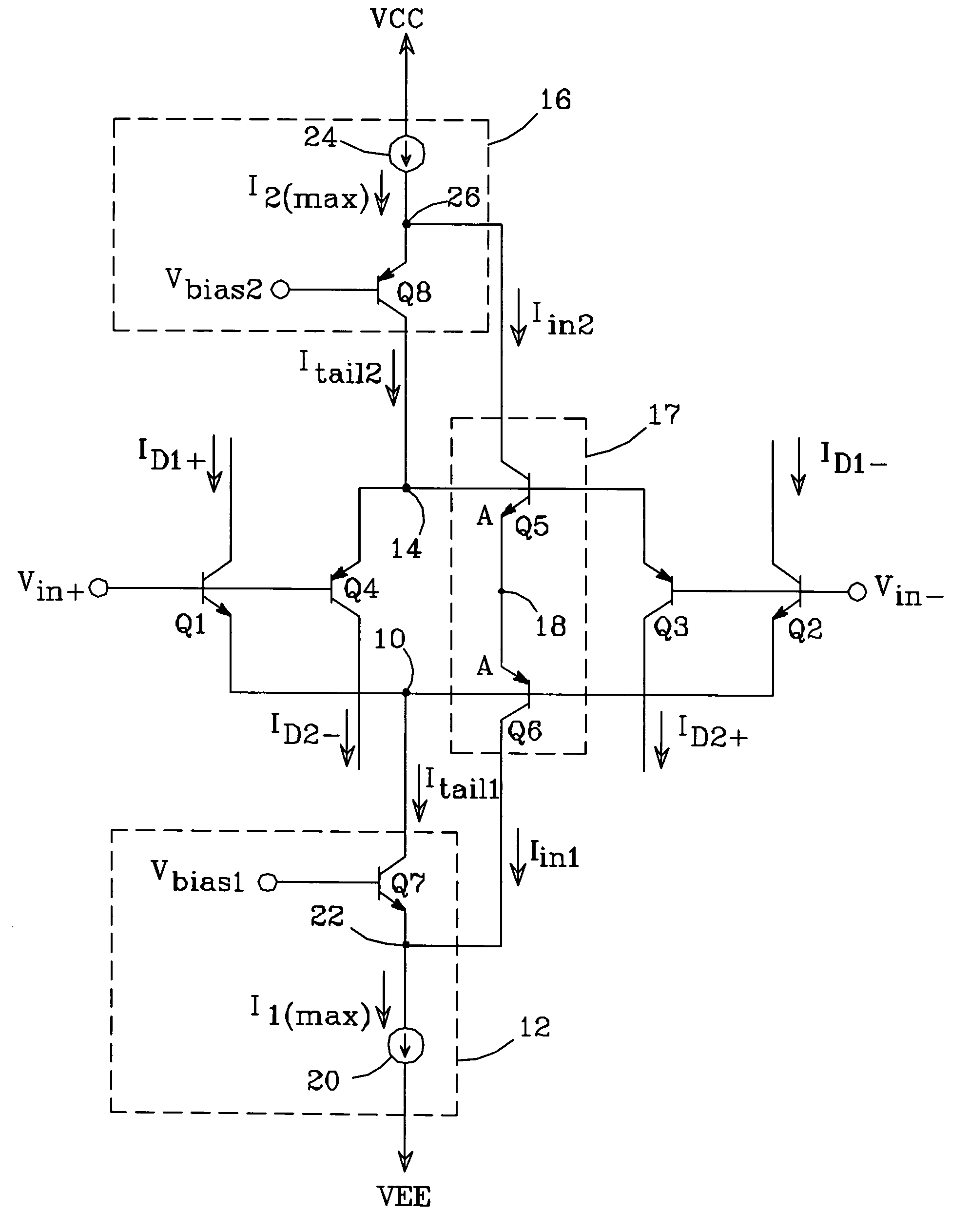
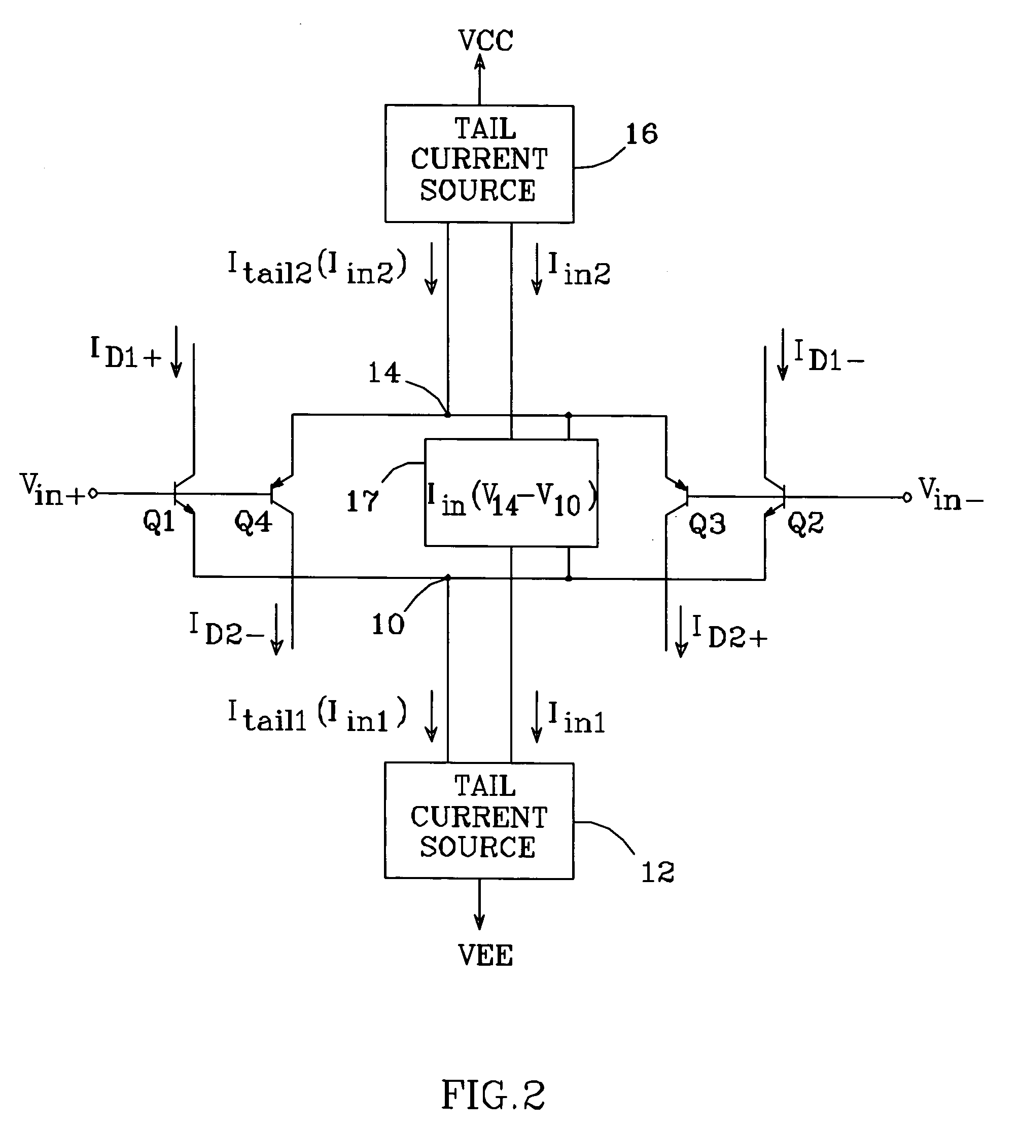
[0026]The basic principles of a common mode linearized input stage per the present invention are shown in FIG. 2. A NPN differential transistor pair Q1 / Q2 have their emitters connected together at a common node 10 and their bases connected to respective input terminals Vin+and Vin−, which receive a differential input signal having a differential voltage Vd. A tail current source 12 provides a tail current Itail1 to common node 10, and Q1 and Q2 conduct respective output currents ID1+and ID1−in response to an applied differential input signal.

[0027]Similarly, a PNP differential transistor pair Q3 / Q4 have their emitters connected together at a common node 14 and their bases connected to input terminals Vin−and Vin+, respectively. A tail current source 16 provides a tail current Itail2 to common node 14, and Q3 and Q4 conduct respective output currents ID2+and ID2−in response to an applied differential input signal.

[0028]The input stage also includes a tail current modulation circuit 1...


PUM


Abstract

A common mode linearized input stage comprises NPN and PNP differential pairs biased with respective tail currents at respective common emitter nodes, with each pair connected to receive a differential input signal. A tail current modulation circuit generates complementary output currents as a function of the voltage difference between the common emitter nodes, and first and second tail current sources generate the tail currents as a function of the complementary output currents. The tail current modulation circuit and the first and second tail current sources are arranged such that the magnitudes of the tail currents increase with an increasing differential input signal.

Description

BACKGROUND OF THE INVENTION[0001]1. Field of the Invention[0002]This invention relates to the field of operational amplifiers (op amps) input stages, and particularly to common mode linearized input stages.[0003]2. Description of the Related Art[0004]The open loop gain of an op amp decreases with increasing input signal frequency. This requires that a larger error signal appear across the amplifier's input for signals of a given amplitude and increasing frequency. This, in turn, requires the op amp to have a large linear input range; if the input range is insufficient, distortion will result.[0005]A bipolar differential transistor pair has a highly nonlinear input range. One way to extend the linear portion of a bipolar pair's input range is with the use of degeneration resistors. However, the use of degeneration resistors can result in noise degradation, as well as loss of headroom.[0006]Another approach to extending linear input range requires the use of class AB-type input stages...

Claims


Application Information

Patent Timeline
Patent Type & Authority Patents(United States)
IPC IPC(8): H03F3/45H03F1/32
CPCH03F1/3211H03F3/45089H03F3/45116H03F3/45484H03F3/4556H03F2203/45366H03F2203/45471
Inventor CARTER, NATHAN R.
Owner ANALOG DEVICES INC
Why Eureka
Try Eureka