Solid-state imaging device, method of manufacturing the same, and electronic apparatus

a solid-state imaging and manufacturing method technology, applied in the direction of radioation control devices, television system scanning details, television systems, etc., can solve the problems of inability to reuse device parameters of related devices, difficulty in ensuring the amount of saturated charges qs, and low performance of surface-type transistors. the effect of sensitivity and dynamic rang

Active Publication Date: 2011-08-04
SONY SEMICON SOLUTIONS CORP
View PDF4 Cites 48 Cited by
  • Summary
  • Abstract
  • Description
  • Claims
  • Application Information

AI Technical Summary

Benefits of technology

[0023]With the solid-state imaging device according to the embodiments of the present invention, since the potentials of the transfer gate electrode extended in a surface of the substrate and the transfer gate electrode buried in the substrate can be independently controlled, an electrical field is created in the vertical direction by an optimal potential applied to the transfer gate electrode buried in the substrate, thereby allowing the charge transfer from the deep position inside of silicon to be improved. Thereby, it is possible to increase the amount of saturated charges Qs per unit area.
[0025]With the electronic apparatus according to the embodiments of the present invention, since the electronic apparatus includes the above-mentioned solid-state imaging device, it is possible to provide an electronic apparatus having a large amount of saturated charges Qs per unit area and a large sensitivity and dynamic range even when the pixel is miniaturized.
[0026]With the three-dimensional transistor according to the embodiments of the present invention, it is possible to control a bidirectional current.

Problems solved by technology

That is, it is difficult to secure the amount of saturated charges Qs.
When the thick gate insulating film is adopted, performance of the surface-type transistor becomes lower than that of the related art, or reuse of device parameters of the transistor of the related art is not possible.
In addition, since the interface between the silicon and the insulation film exists in under the periphery of the vertical transfer transistor, white spots are deteriorated by the generation of a dark current from the interface thereof.
Further, when non-doped polysilicon which is a gate electrode material for a peripheral CMOS circuit formed by a general dual gate process is used in the vertical electrode at the time of forming the vertical transistor, it cannot be made conductive only by impurity doping through ion implantation and thermal diffusion to a certain degree of depth or more.
In addition, attachment and detachment of the electrode material lead to an increase in the number of processes, and cause deterioration of the processing yield.

Method used


Image

  • Solid-state imaging device, method of manufacturing the same, and electronic apparatus
  • Solid-state imaging device, method of manufacturing the same, and electronic apparatus
  • Solid-state imaging device, method of manufacturing the same, and electronic apparatus

Examples


first embodiment

Operation of First Embodiment

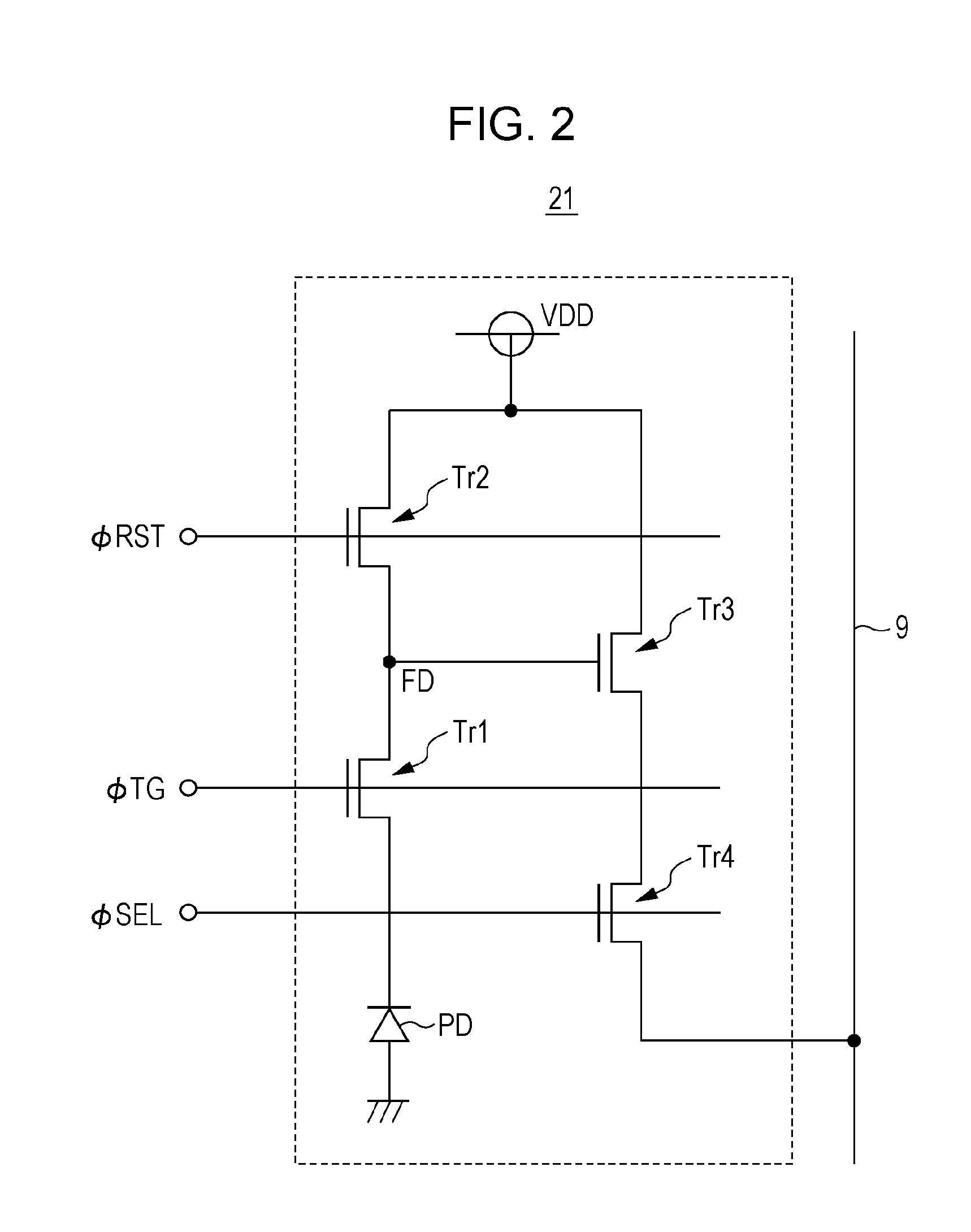
[0083]An operation of the solid-state imaging device 31 according to the first embodiment will be described. The solid-state imaging device 31 of the embodiment has the photodiode PD (PD1, PD2) with a two-stage structure in the depth direction of the semiconductor substrate (that is, p-type semiconductor well region 33). In the case of this photodiode PD with a two-stage structure, two charge transfers are performed as the charge transfer. That is, two charge transfers are performed on one lateral direction transfer in which the charge transfer is performed from the surface-side photodiode PD1 to the floating diffusion portion, and the other longitudinal direction transfer in which the other charge transfer is performed from the embedded-side photodiode PD2 toward the channel region generated by the transfer gate electrode extended in a surface of the substrate. The same is true of the multistage photodiode PD. That is, herein performed are two charge tr...

example 1

of Method of Manufacturing Solid-State Imaging Device

[0113]FIGS. 11A and 11B and FIGS. 12A and 12B show an example of the method of manufacturing the solid-state imaging device 31 according to the first embodiment. First, as shown in FIG. 11A, the separation region 37 (not shown) and the photodiode PD (D1, PD2) are formed in the p-type semiconductor well region 33 of the semiconductor substrate. In addition, the other pixel transistors are formed by the plane transistor which includes the floating diffusion portion (FD) and has a plane gate electrode in the pixel transistor. In this case, in the transfer transistor Tr1, the plane transfer transistor is also formed simultaneously with other pixel transistors except for the vertical transistor described later. In this plane transfer transistor, the transfer gate electrode 42 extended in a surface of the substrate is formed on the surface of the p-type semiconductor well region 33 with the gate insulating film 41a interposed therebetwe...

example 2

of Method of Manufacturing Solid-State Imaging Device

[0119]FIGS. 13A and 13B and FIGS. 14A and 14B show an example of the method of manufacturing the solid-state imaging device 31 according to the first embodiment. First, as shown in FIG. 13A, FIGS. 11A and 11B and FIGS. 12A and 12B show an example of the method of manufacturing the solid-state imaging device 31 according to the first embodiment. First, as shown in FIG. 11A, the separation region 37 (not shown) and the photodiode PD (D1, PD2) are formed in the p-type semiconductor well region 33 of the semiconductor substrate. In addition, the other pixel transistors are formed by the plane transistor which includes the floating diffusion portion (FD) and has a plane gate electrode in the pixel transistor. In this case, in the transfer transistor Tr1, the plane transfer transistor is also formed simultaneously with other pixel transistors except for the vertical transistor described later. In this plane transfer transistor, the tran...


PUM


Abstract

A solid-state imaging device is provided, which includes a pixel region in which pixels including a photoelectric conversion section and a plurality of pixel transistors are arranged. In the solid-state imaging device, a transfer transistor of the pixel transistors includes: a transfer gate electrode extended in a surface of the substrate formed on the surface of a semiconductor substrate; and a transfer gate electrode buried in the substrate which is electrically insulated from the transfer gate electrode extended in a surface of the substrate and is embedded in the inside of the semiconductor substrate in the vertical direction through the transfer gate electrode extended in a surface of the substrate.

Description

BACKGROUND OF THE INVENTION[0001]1. Field of the Invention[0002]The present invention relates to a solid-state imaging device, a method of manufacturing the same, and an electronic apparatus, such as a camera, including the solid-state imaging device.[0003]2. Description of the Related Art[0004]CMOS solid-state imaging devices are known as solid-state imaging devices. This CMOS solid-state imaging device is configured such that one pixel is formed by a photodiode and a plurality of pixel transistors, and a plurality of pixels is two-dimensionally arranged. This photodiode is a photoelectric conversion element that generates and accumulates signal charges in response to the amount of light received, and a plurality of pixel transistors is an element that transfers the signal charges from the photodiode, and reads out the signal charges as a signal. A plurality of pixel transistors can include, for example, four MOS transistors such as a transfer transistor, a reset transistor, an amp...

Claims


Application Information

Patent Timeline
Patent Type & Authority Applications(United States)
IPC IPC(8): H04N5/335H01L27/148H01L31/18H01L29/78
CPCH01L27/14812H01L29/7813H04N5/374H01L27/146H01L27/148H04N5/335H01L29/78H01L27/14614H01L27/14638H01L27/14641H01L27/1464H01L27/14647H04N25/626H04N25/60H04N25/76
Inventor SHINOHARA, TAKEKAZU
Owner SONY SEMICON SOLUTIONS CORP
Why Eureka
Try Eureka