Nonvolatile memory, semiconductor device, and method of programming to nonvolatile memory

Inactive Publication Date: 2005-11-08
RENESAS ELECTRONICS CORP
View PDF10 Cites 41 Cited by
  • Summary
  • Abstract
  • Description
  • Claims
  • Application Information

AI Technical Summary

Benefits of technology

[0019]Preferably, the application time of the write voltage is determined on the basis of a clock signal, and the cycle of the clock signal is changed to thereby change the application time of the write voltage. Consequently, the change in the application time of the write voltage can be realized by the simple method of changing the cycle of the clock signal. More concretely, a variable frequency dividing circuit capable of generating the clock signals of different cycles on the basis of a reference clock signal and a register for setting a value of designating a frequency dividing ratio in the variable frequency dividing circuit are provided. By changing the frequency driving ratio, the cycle of the clock signal is changed. With the configuration,

Problems solved by technology

However, since the writing operation is performed (write cycle is included) even in the case where write data is “1” and it is unnecessary to apply a voltage, time is wasted.
Consequently, in the case where a booster c

Method used


Image

  • Nonvolatile memory, semiconductor device, and method of programming to nonvolatile memory
  • Nonvolatile memory, semiconductor device, and method of programming to nonvolatile memory
  • Nonvolatile memory, semiconductor device, and method of programming to nonvolatile memory

Examples


Embodiment Construction

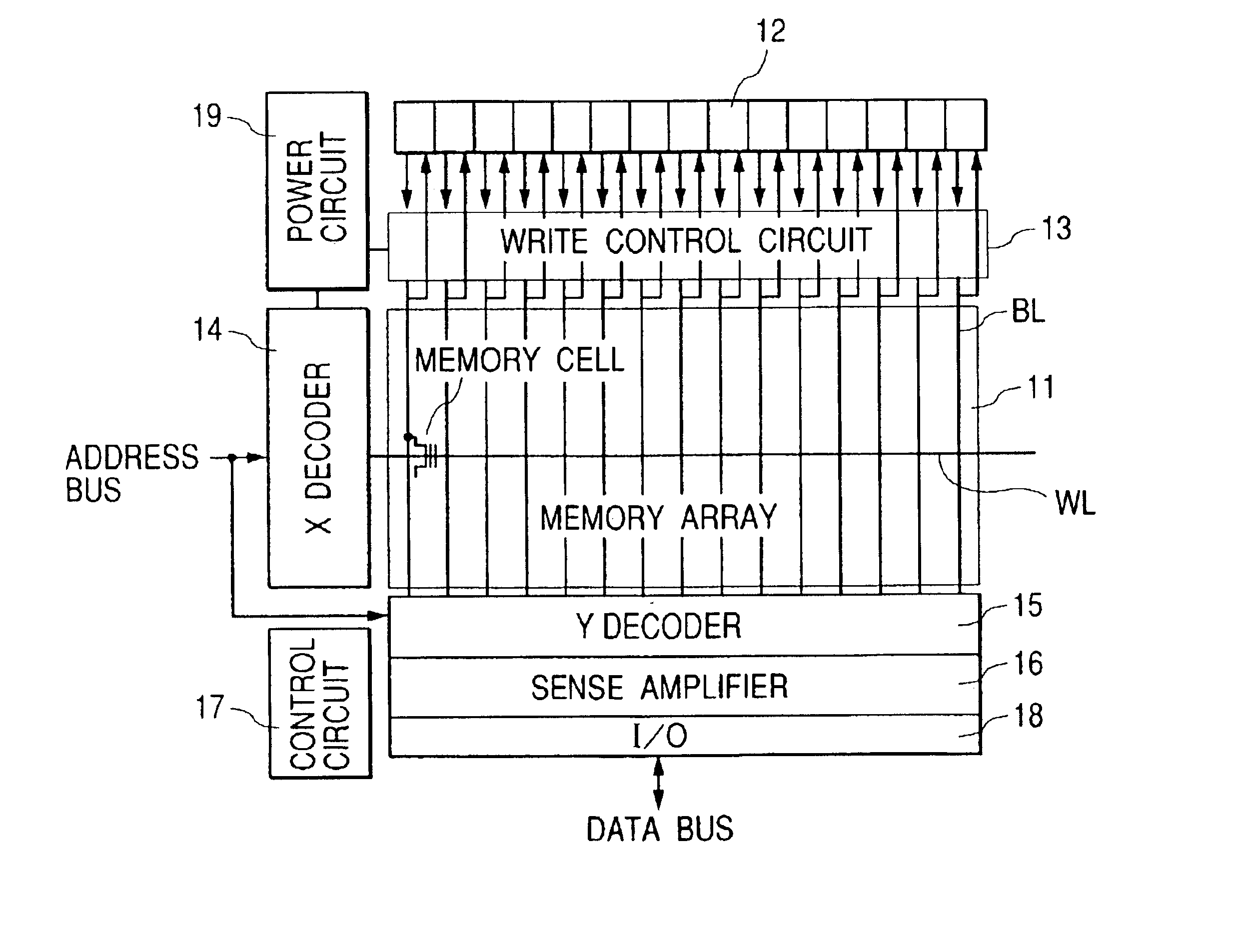
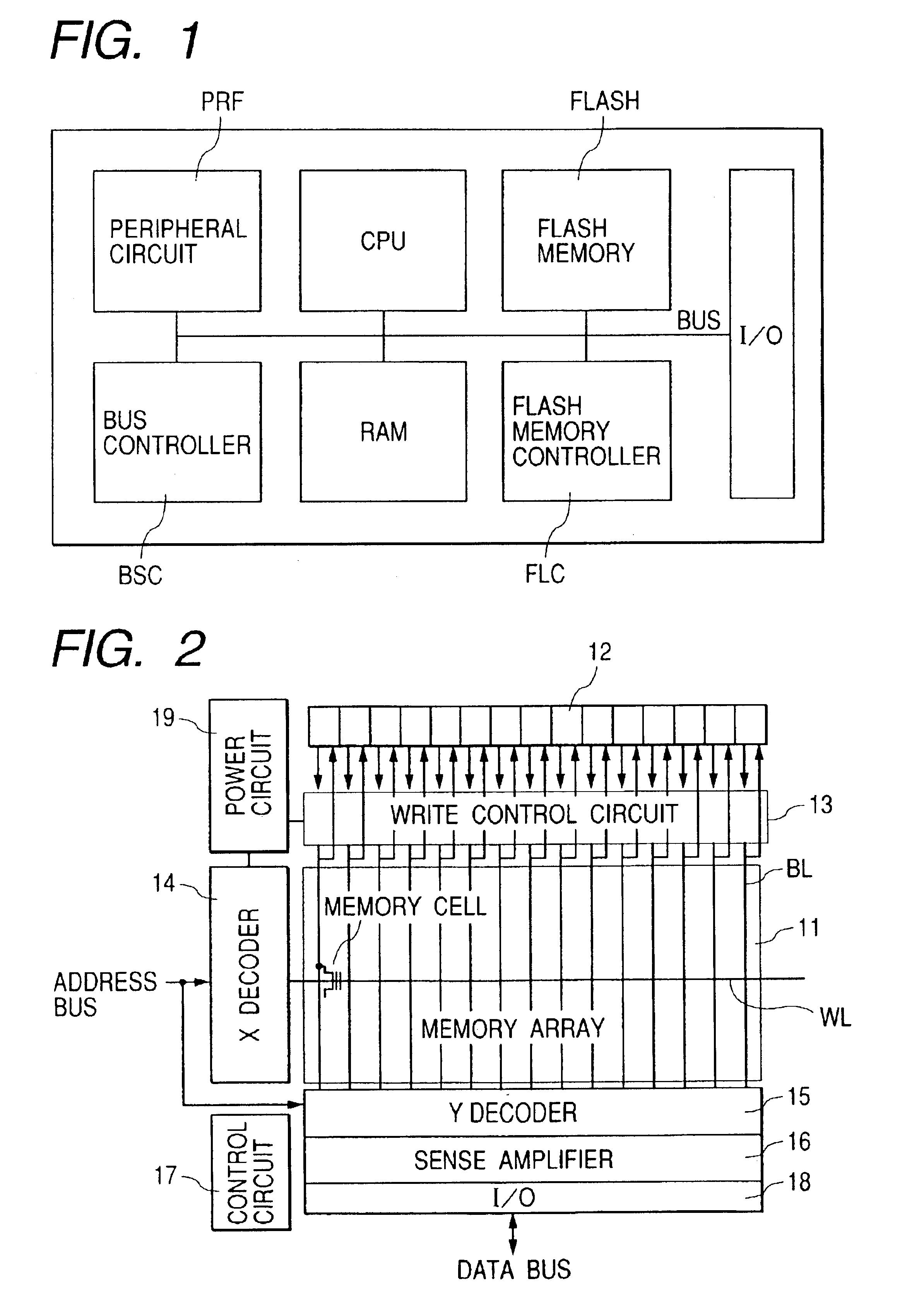
[0051]Embodiments of the invention will be described herein below with reference to the drawings. FIG. 1 shows a schematic configuration of a microcomputer having therein a flash memory to which the invention is applied (herein below, called a flash memory integrated microcomputer). Although not limited, circuit blocks shown in FIG. 1 are formed on a single semiconductor chip made of single crystal silicon or the like.

[0052]Shown in FIG. 1 are: a flash memory FLASH having a memory array in which memory cells each constructed by an MOSFET having a control gate and a floating gate are arranged in a matrix; a flash controller FLC for writing and erasing data to / from the flash memory; a central processing unit CPU for controlling the whole chip; a random access memory RAM for temporarily storing data and providing a work area of the central processing unit CPU; a peripheral circuit PRP such as various timers, an A / D converter, and a watchdog timer for monitoring the system; an internal ...


PUM


Abstract

Disclosed is a nonvolatile memory with a shortened total write time, capable of stably writing data by making a write current constant while reducing fluctuations in a voltage generated by a booster circuit. In a nonvolatile memory such as a flash memory, data is determined at the time of writing operation. While skipping a bit corresponding to write data having the logic “1” (or logic “0”), writing operation to bits corresponding to write data having the logic “0” (or logic “1) is successively performed.

Description

[0001]This application is a continuation of Ser. No. 09 / 964,394 filed Sep. 28, 2001, now a U.S. Pat. No. 6,567,313.BACKGROUND OF THE INVENTION[0002]The present invention relates to a technique effective for application to a method of applying a write voltage in an electrically erasable programmable nonvolatile memory, and a technique effective for use in a flash memory capable of erasing data in a lump, for example, on a block unit basis and a microcomputer having therein the flash memory.[0003]A flash memory uses a nonvolatile memory cell taking the form of a MOSFET of a two-layer gate structure having a control gate and a floating gate, and a memory cell can be constructed by a single transistor. Conventional methods of writing data into a flash memory include a method of changing a threshold voltage by injecting or discharging charges to / from a floating gate by using an FN tunnel phenomenon by applying a voltage across the control gate and a substrate (what is called a well regio...

Claims


Application Information

Patent Timeline
IPC IPC(8): G11C16/06G11C16/12G11C16/02G11C8/02
CPCG11C16/12G11C16/3459G11C2216/14G11C16/02
Inventor TANAKA, TOSHIHIROSHINAGAWA, YUTAKASUZUKAWA, KAZUFUMIFUJITO, MASAMICHIYAMAKI, TAKASHIMAKUTA, KIICHIWADA, MASASHIKAWAJIRI, YOSHIKI
Owner RENESAS ELECTRONICS CORP
Why Eureka
Try Eureka