Array of gate dielectric structures to measure gate dielectric thickness and parasitic capacitance

a gate dielectric capacitor and parasitic capacitance technology, applied in the field of manufacturing semiconductor devices, can solve the problems of inability to accurately measure the capacitance of ultra-thin gate dielectric capacitors, too slow device speed, and short circuiting, etc., to achieve accurate measurement of the capacitance of gate dielectric capacitors and eliminate parasitic capacitance

Inactive Publication Date: 2005-11-15
GLOBALFOUNDRIES INC
View PDF22 Cites 15 Cited by
  • Summary
  • Abstract
  • Description
  • Claims
  • Application Information

AI Technical Summary

Benefits of technology

[0015]This invention addresses the needs for an improved method of measuring the capacitance and gate dielectric thickness of ultra-thin gate dielectric capacitors. The present invention eliminates parasitic capacitance from the gate dielectric capacitance measurements enabling accurate measurement of the gate dielectric capacitor capacitance.

Problems solved by technology

If the gate dielectric thickness is too thin, short-circuiting is a problem.
If the gate dielectric layer is too thick, then the device speed will be too slow.
The capacitance of large area, ultra-thin gate dielectric capacitors cannot be accurately measured directly.
The large area gate dielectric capacitors tend to suffer from high gate leakage through the gate.
The capacitance of small area gate dielectric capacitors also cannot be directly measured with accuracy.
Gate leakage does not appreciably hinder measuring the capacitance of small area gate dielectric capacitors, rather parasitic capacitance interferes with accurate gate dielectric capacitance measurements in small area gate dielectric capacitors.

Method used


Image

  • Array of gate dielectric structures to measure gate dielectric thickness and parasitic capacitance
  • Array of gate dielectric structures to measure gate dielectric thickness and parasitic capacitance
  • Array of gate dielectric structures to measure gate dielectric thickness and parasitic capacitance

Examples


Embodiment Construction

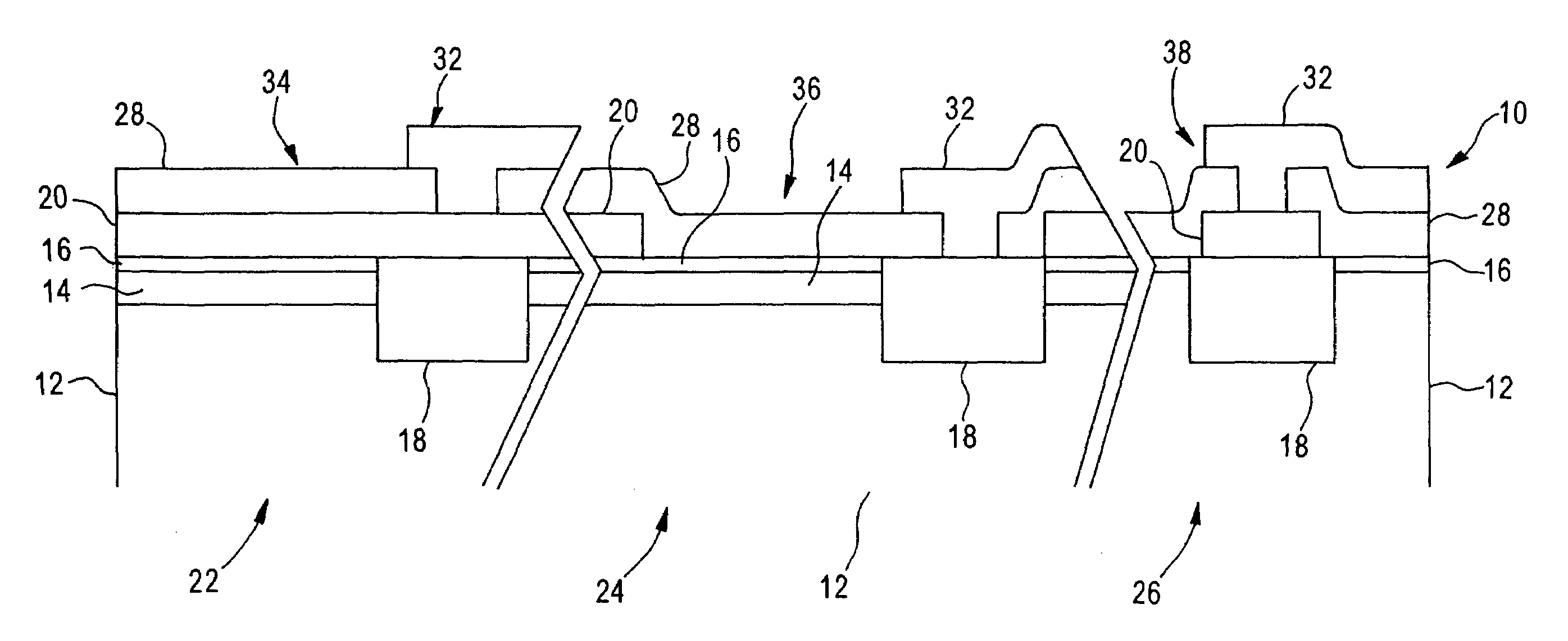
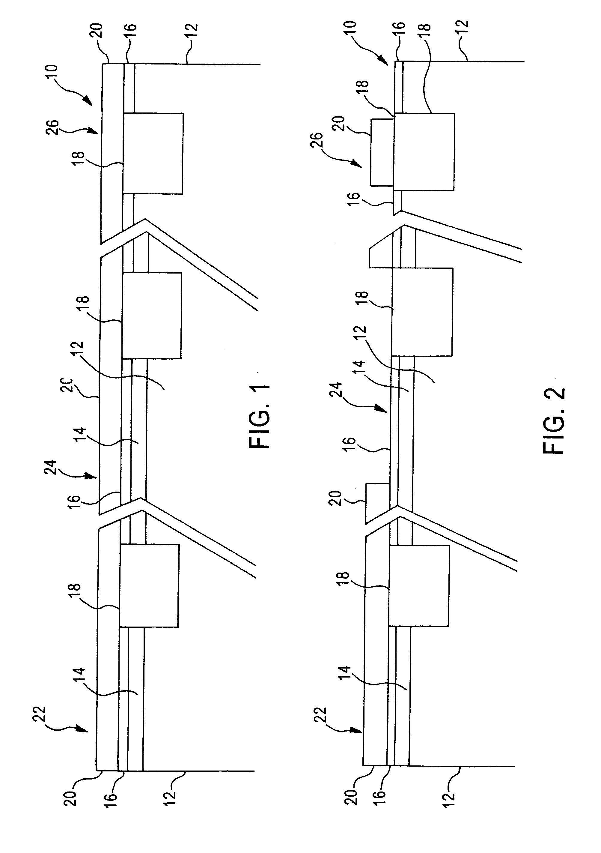
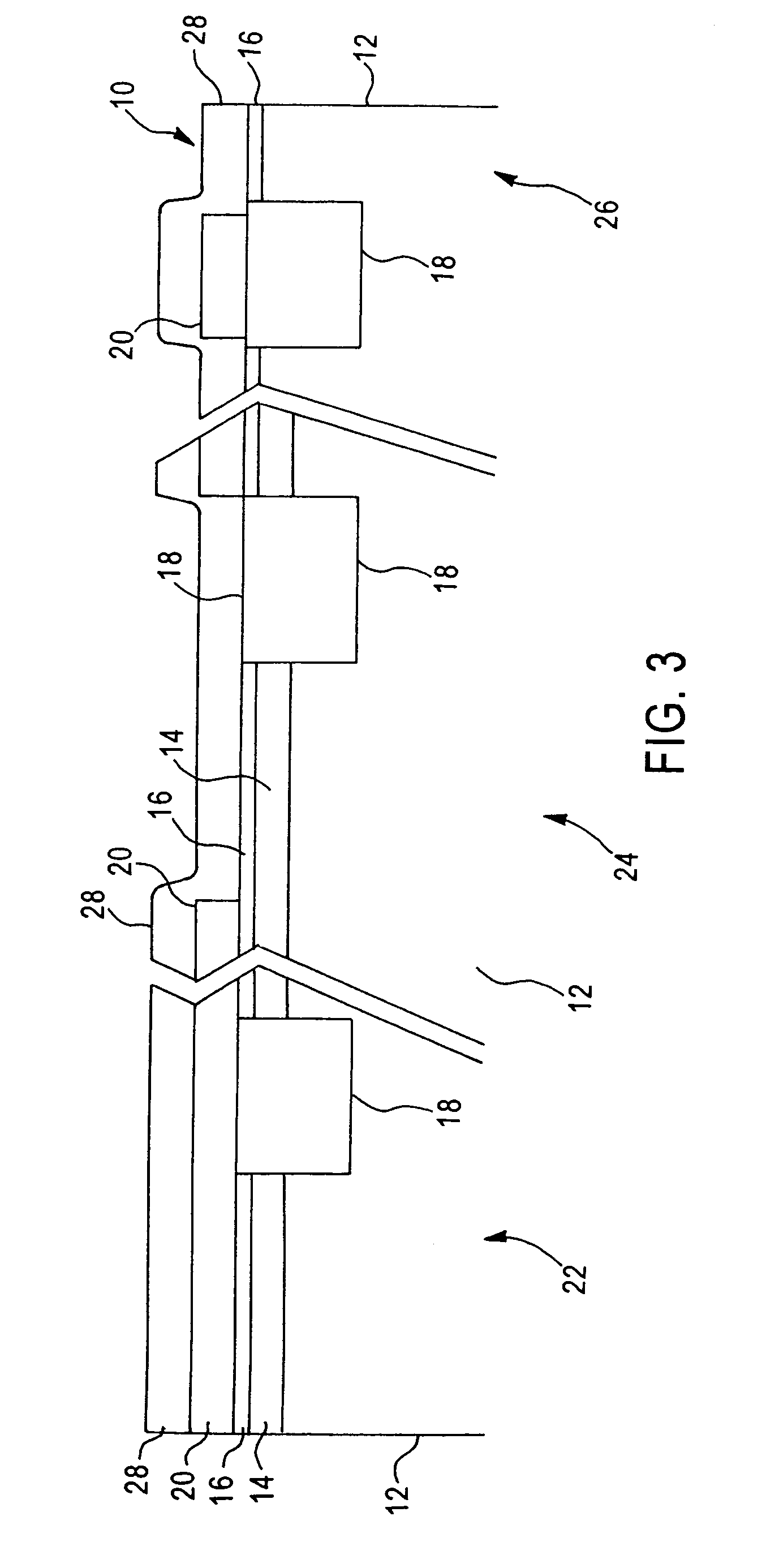
[0021]The present invention enables the accurate measurement of the gate dielectric thickness in ultra-thin gate dielectric capacitors. A wafer is provided with dummy structures and a method for eliminating parasitic capacitance from gate dielectric capacitance measurements. The present invention uses two different types of dummy structures so that the parasitic capacitance can be measured and subtracted from the total capacitance of gate dielectric capacitors. The two types of dummy structures that are formed are substantially similar to gate dielectric capacitor devices formed on the wafer, with the exception that the first type of dummy structure does not include one of the capacitor electrodes and the second type of dummy structure does not include the other capacitor electrode.

[0022]The invention will be described in conjunction with the formation of a gate dielectric capacitor and first and second dummy structures, as shown in the accompanying drawings. However, this is exempl...


PUM


Abstract

Accurate determination of gate dielectric thickness is required to produce high-reliability and high-performance ultra-thin gate dielectric semiconductor devices. Large area gate dielectric capacitors with ultra-thin gate dielectric layers suffer from high gate leakage, which prevents the accurate measurement of gate dielectric thickness. Accurate measurement of gate dielectric thickness of smaller area gate dielectric capacitors is hindered by the relatively large parasitic capacitance of the smaller area capacitors. The formation of first and second dummy structures on a wafer allow the accurate determination of gate dielectric thickness. First and second dummy structures are formed that are substantially similar to the gate dielectric capacitors except that the first dummy structures are formed without the second electrode of the capacitor and the second dummy structures are formed without the first electrode of the capacitor structure. The capacitance, and therefore thickness, of the gate dielectric capacitor is determined by subtracting the parasitic capacitances measured at the first and second dummy structures.

Description

[0001]This application is a divisional of application Ser. No. 10 / 021,497 filed Dec. 19, 2001, now U.S. Pat. No. 6,841,832.TECHNICAL FIELD[0002]The present invention relates to the field of manufacturing semiconductor devices and, more particularly, to an improved method of measuring gate dielectric thickness and parasitic capacitance.BACKGROUND OF THE INVENTION[0003]An important aim of ongoing research in the semiconductor industry is the reduction in the dimensions of semiconductor devices. Planar transistors such as metal oxide semiconductor field effect transistors (MOSFET), are particularly well suited for use in high-density integrated circuits. As the size of the MOSFET and other active devices decreases, the dimensions of the gate electrodes and gate dielectric layers decrease correspondingly. Tight control of the gate dielectric thickness is necessary to manufacture reduced-size, high-reliability, high-speed transistors.[0004]Gate dielectric capacitors are commonly used in ...

Claims


Application Information

Patent Timeline
Patent Type & Authority Patents(United States)
IPC IPC(8): H01L29/66H01L29/76H01L21/66H01L31/115H01L31/119H01L21/8234H01L23/544H01L27/08
CPCH01L21/823437H01L22/34H01L27/0811H01L2924/0002H01L2924/00
Inventor EN, WILLIAM G.MICHAEL, MARK W.WANG, HAI HONGCHAN, SIMON SIU-SING
Owner GLOBALFOUNDRIES INC
Why Eureka
Try Eureka