Method of base formation in a BiCMOS process

a bicmos and process technology, applied in the field of bipolar transistors, can solve the problems of device performance degradation, serious device operational limitations, and inability to meet the requirements of the base region

Inactive Publication Date: 2005-11-15
INT BUSINESS MASCH CORP
View PDF20 Cites 16 Cited by
  • Summary
  • Abstract
  • Description
  • Claims
  • Application Information

AI Technical Summary

Benefits of technology

[0013]An object of the present invention is to provide simple, yet practical methods of fabricating a high-performance HBT in an integrated BiCMOS process.
[0014]A further object of the present invention is to provide methods of forming a HBT having a raised extrinsic base in which base resistance is further lowered as compared to a conventional HBT having a raised extrinsic base.

Problems solved by technology

As the vertical dimensions of the bipolar transistor are scaled more and more, serious device operational limitations have been encountered.
The ion implantation will cause damage, however, to the base region.
Such damage may ultimately lead to degradation in device performance.

Method used


Image

  • Method of base formation in a BiCMOS process
  • Method of base formation in a BiCMOS process
  • Method of base formation in a BiCMOS process

Examples


first embodiment

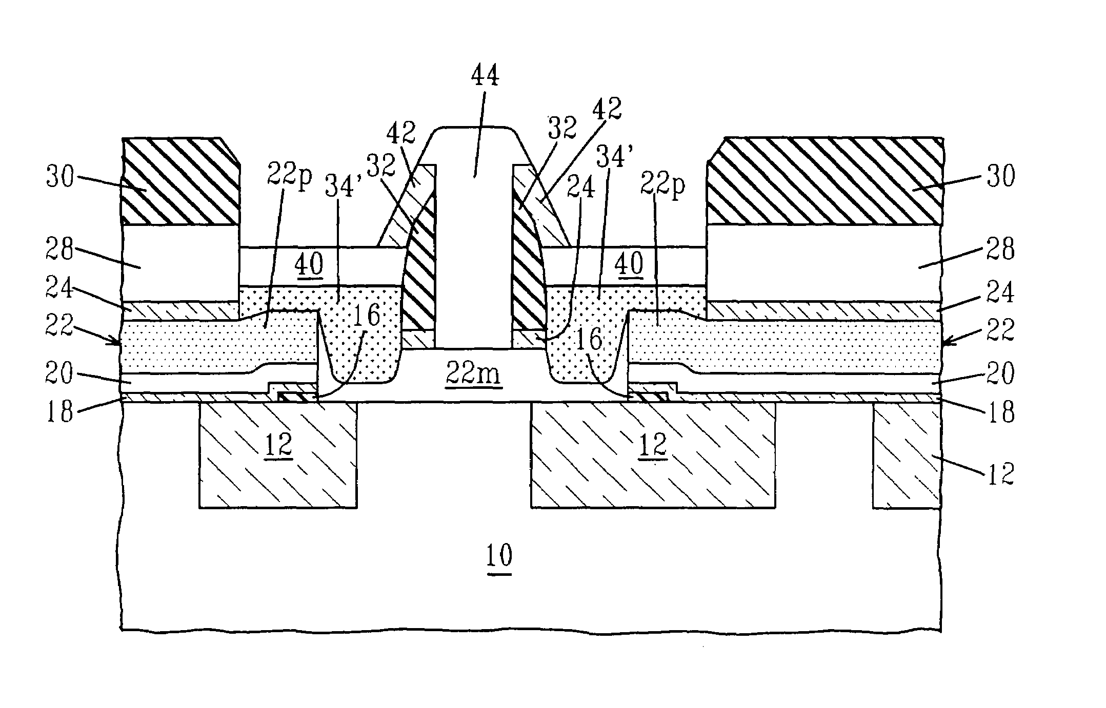
[0059]It is noted that in the structure shown, for example, in FIG. 11, the silicide region 40 atop the raised extrinsic base extends to the emitter 44 in a self-aligned manner and the silicide 40 exhibits improved, e.g., lowered, resistivity characteristics. Moreover, the silicide 40 is produced in the present invention such that substantially little or no agglomeration occurs.

[0060]As stated above, FIGS. 1–11 show the processing steps that are employed in a first embodiment of the present invention. In the first embodiment of the present invention, the silicide region is formed prior to emitter formation. As shown in FIG. 11, an inner edge of the silicide region 40 is in contact with the insulating spacers 32 which isolate the silicide region 40 from the emitter 44. In addition to the first embodiment depicted above, the present invention also contemplates a second method of forming a HBT structure having the extrinsic base silicide (i.e., silicide region 40) formed in a self-alig...

second embodiment

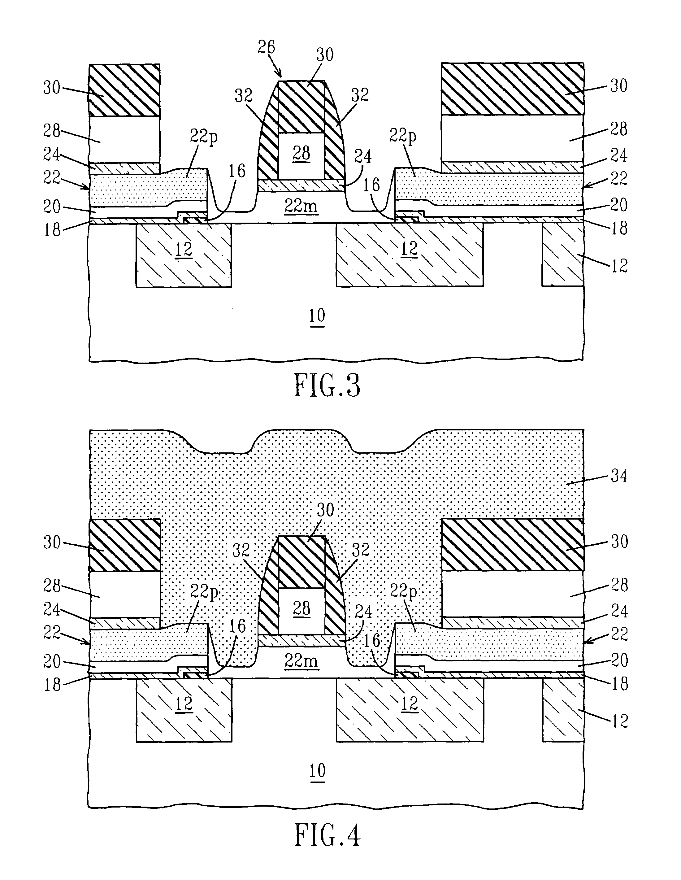
[0064]Next, the nitride layers are opened by chemical mechanical polishing (CMP) or etching utilizing oxide layer 29 as a polish stop layer or an etch stop layer. The resultant structure formed after this step of the present invention has been performed is shown, for example, in FIG. 15. In the structure shown in FIG. 15, the upper surface layer now comprises nitride that is located above the raised extrinsic base 34″ and oxide layer 29.

[0065]The oxide layer 29 that is exposed in FIG. 15 together with the underlying polysilicon layer 28 of the emitter pedestal region 26 are then removed by reactive ion etching or wet chemical etching to provide the structure shown in FIG. 16. In FIG. 16, oxide layer 24 of the emitter pedestal region 26 that lies above the monocrystalline 22m base region 22 is exposed.

[0066]Next, and as shown in FIG. 17, emitter polysilicon 44 and a nitride cap 45 are deposited and the structure is patterned by lithography and etching. In this step of the present inv...


PUM


Abstract

Methods for fabricating a heterojunction bipolar transistor having a raised extrinsic base is provided in which the base resistance is reduced by forming a silicide atop the raised extrinsic base that extends to the emitter region in a self-aligned manner. The silicide formation is incorporated into a BiCMOS process flow after the raised extrinsic base has been formed. The present invention also provides a heterojunction bipolar transistor having a raised extrinsic base and a silicide located atop the raised extrinsic base. The silicide atop the raised extrinsic base extends to the emitter in a self-aligned manner. The emitter is separated from the silicide by a spacer.

Description

BACKGROUND OF INVENTION[0001]1. Field of the Invention[0002]The present invention relates generally to a bipolar transistor and, more particularly to methods for forming a bipolar transistor with a raised extrinsic base in an integrated bipolar and complementary metal oxide semiconductor (BiCMOS) transistor circuit in which the base resistance is lowered by extending the raised extrinsic base silicide to the emitter region in a self-aligned manner.[0003]2. Background of the Invention[0004]Bipolar transistors are electronic devices with two p-n junctions that are in close proximity to each other. A typical bipolar transistor has three device regions: an emitter, a collector, and a base disposed between the emitter and the collector. Ideally, the two p-n junctions, i.e., the emitter-base and collector-base junctions, are in a single layer of semiconductor material separated by a specific distance. Modulation of the current flow in one p-n junction by changing the bias of the nearby ju...

Claims


Application Information

Patent Timeline
Patent Type & Authority Patents(United States)
IPC IPC(8): H01L21/28H01L21/331H01L29/417H01L29/737H01L29/732H01L29/66H01L29/40H01L21/70H01L21/02H01L21/8249H01L31/102H01L21/8222H01L31/072H01L29/73H01L27/06H01L31/06H01L31/109H01L21/8248
CPCH01L21/28518H01L21/8249H01L27/0623H01L29/7371H01L29/456H01L29/66242H01L29/0804
Inventor GEISS, PETER J.KHATER, MARWAN H.LIU, QIZHIMANN, RANDY W.PURTELL, ROBERT J.RAINEY, BETHANNRIEH, JAE-SUNGSTRICKER, ANDREAS D.
Owner INT BUSINESS MASCH CORP
Why Eureka
Try Eureka