Methods and systems for detecting defective imaging pixels and pixel values

a technology of defective imaging pixels and pixel values, applied in the field of imaging devices, can solve the problems of only correcting the identified bad pixels using conventional techniques, destroying edges, and detecting bad pixels and bad pixel values, so as to prevent the loss of edges, reduce the need for bad pixel look up tables, and reduce the effect of high frequency conten

Inactive Publication Date: 2005-11-15
YOULIZA GEHTS LIABILITY
View PDF19 Cites 93 Cited by
  • Summary
  • Abstract
  • Description
  • Claims
  • Application Information

AI Technical Summary

Benefits of technology

[0014]One significant advantage of the present invention is that the correction or compensation for some or all bad pixels may be performed, including bad pixels and bad pixel values that are introduced during the real-time operation of the imaging system due to temperature and/or gain changes. Thus, bad pixels and bad pixel values may be detected while the imaging device is used on-line by a consumer or other end-user, such as in a camera or the like. By contrast, conventional techniques only correct bad pixels that were identified during the manufacturing process, before the imaging device is delivered to the end-user.
[0015]Another significant advantage of the present system is that it prevents the loss of edges in a reconstructed image. Conventional processes may destroy edges via the correction process since often times the correction involves a low pass filter that reduces the high frequency content of the reconstructed image.
[0016]Still another advantage of the present system is that, because the present invention corrects bad pixels on-line, the need for bad pixel look up tables is reduced or eliminated. Thus, the cost and complexity associated with non-volatile storage units conventional used to store bad pixel lookup tables, such as those used by conventional systems is reduced or eliminated. Also, the system is advantageously able to correct individual bad pixels distributed randomly in an array, rather than solely a cluster or column of bad pixels.
[0017]In one embodiment, the imaging syste

Problems solved by technology

Thus, bad pixels and bad pixel values may be detected while the imaging device is used on-line by a consumer or other end-user, such as in a camera or the like.
By contrast, conventional techniques only correct bad pixels that were identified during the manufactur

Method used


Image

  • Methods and systems for detecting defective imaging pixels and pixel values
  • Methods and systems for detecting defective imaging pixels and pixel values
  • Methods and systems for detecting defective imaging pixels and pixel values

Examples


Embodiment Construction

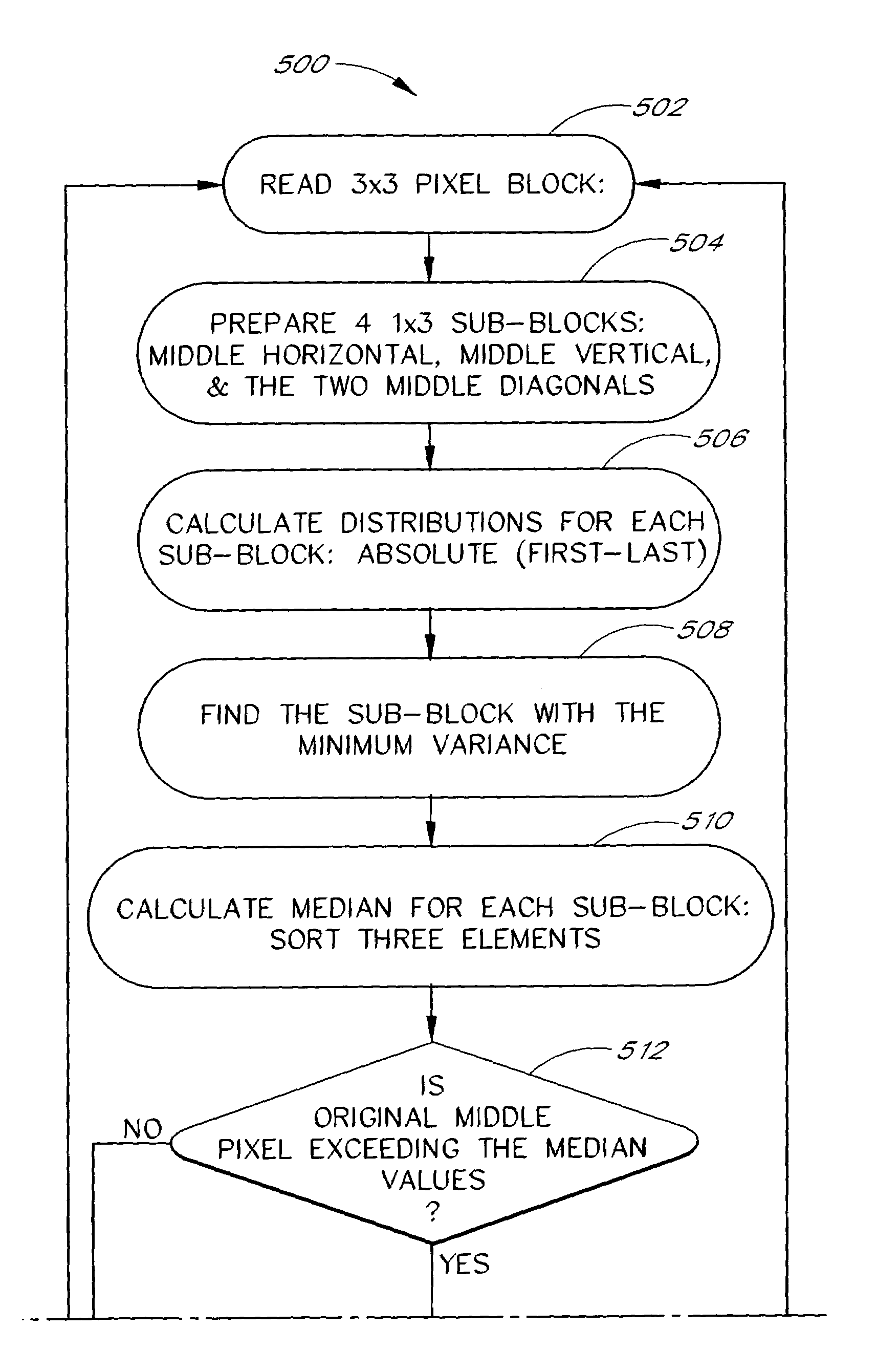
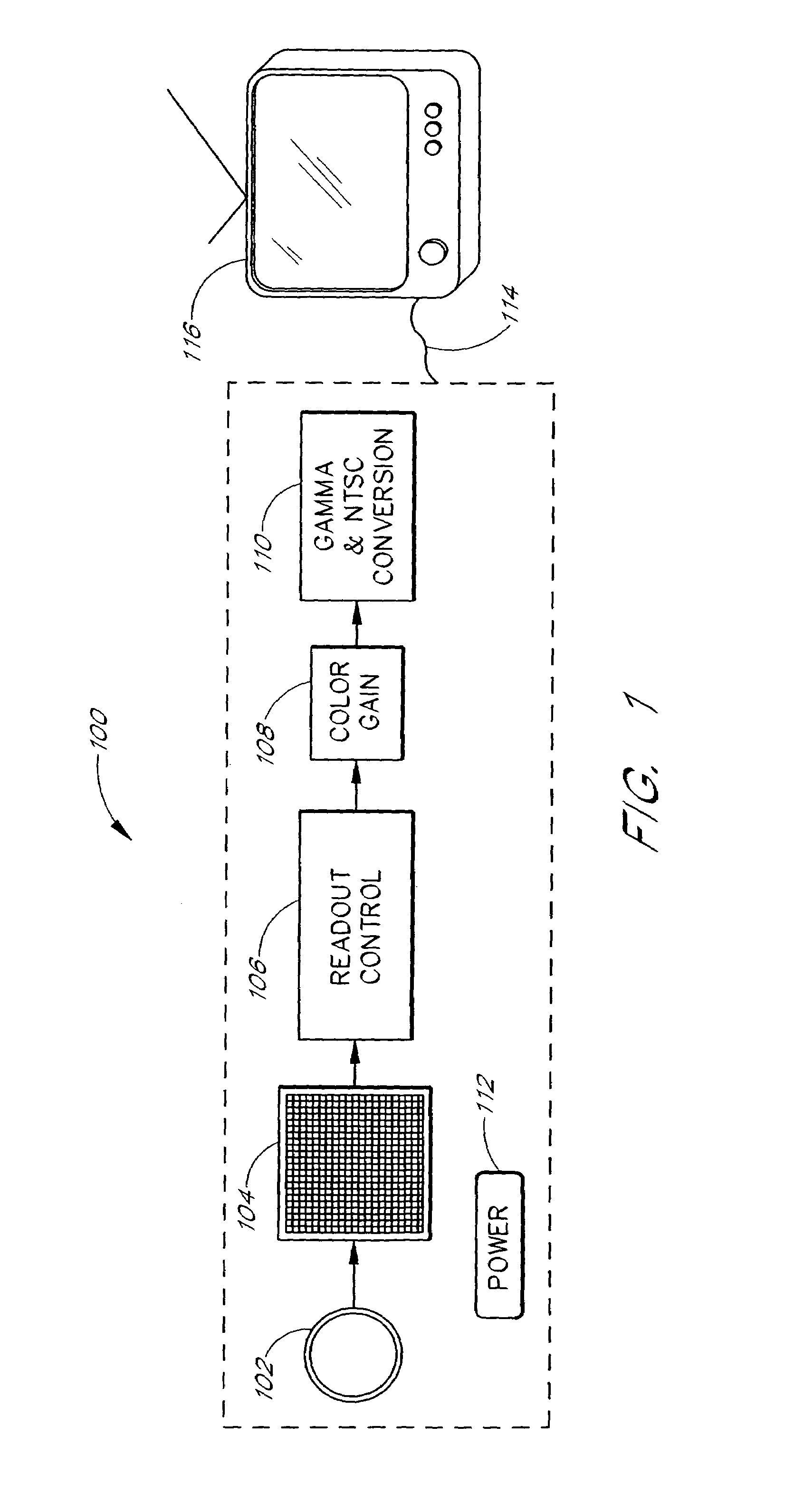
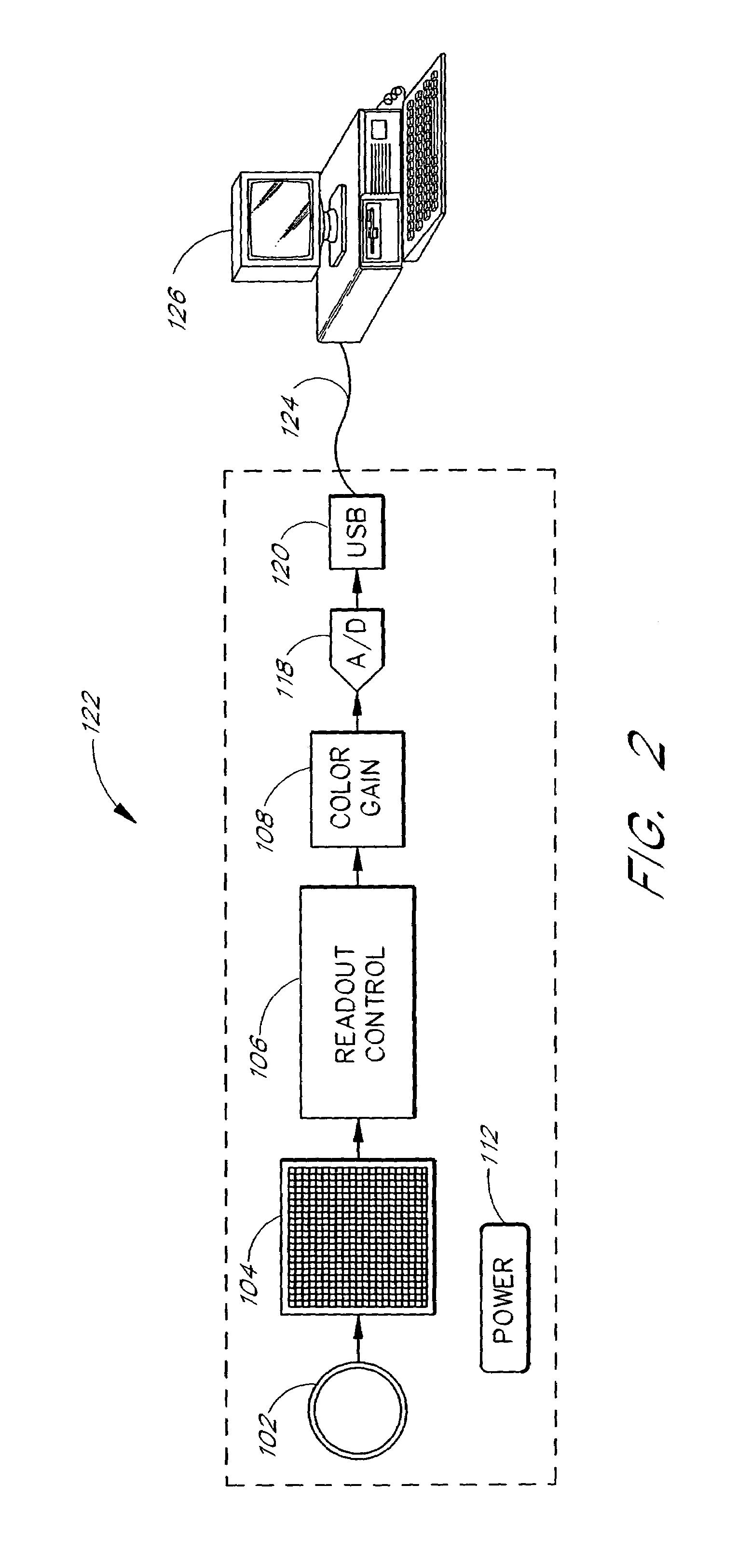
[0033]The present invention relates to a novel imaging system that provides flexible addressing and processing of imaging pixel sensor elements. The novel architecture of the present invention allows for a highly integrated, low cost imager with high speed performance and good image quality. Defective or bad pixels within an array of active or passive pixel sensor cells are detected and compensated for, thereby reducing or eliminating the visible effects the bad pixels may have on resulting images. In one embodiment, the imaging system provides an on-line, on-the-fly bad pixel detection and correction process that provides high speed operation, reduced non-volatile storage requirements, and good performance.

[0034]For example, one embodiment of the present invention provides an on-line bad pixel detection and correction process and circuit that compares a first pixel readout value with another value derived at least in part on the readout values of other pixels in first pixel's local...


PUM


Abstract

The present invention is related to methods and systems for detecting defective imaging array pixels and providing correction, thereby reducing or eliminating visible image artifacts. One embodiment of the present invention provides an on-line bad pixel detection and correction process that compares a first pixel readout value with a first value related to the readout values of other pixels in first pixel's local neighborhood. When the first pixel readout value varies by more than a first amount as compared with the first value, a second value related to the readout values of the neighboring pixels is used in place of the first pixel readout value.

Description

CLAIM OF PRIORITY[0001]This patent application claims the benefit of U.S. Provisional Application No. 60 / 149,796 filed Aug. 19, 1999, and U.S. application Ser. Nos. 09 / 495,971, 09 / 496,364, 09 / 496,533, 09 / 496,607, filed Feb. 2, 2000, which are hereby incorporated herein by reference in their entirety.BACKGROUND OF THE INVENTION[0002]1. Field of the Invention[0003]The present invention relates to imaging devices and, more particularly, to methods and systems for compensating for defective pixels and pixel values.[0004]2. Description of the Related Art[0005]Conventional integrated circuit imaging devices include an array of light detecting elements or pixels which are interconnected to generate an analog signal representation of an image illuminating the device. Two common examples of conventional integrated circuit imaging devices are a charge coupled device (CCD) and a complementary metal oxide semiconductor (CMOS) image sensing device. Conventional imaging devices typically include ...

Claims


Application Information

Patent Timeline
IPC IPC(8): H04N9/44H04N9/64H04N9/47H04N7/18H04N5/367H04N5/378H04N9/07
CPCH04N5/3675H04N9/045H04N25/683H04N23/843H04N25/134
Inventor NETER, SARIT
Owner YOULIZA GEHTS LIABILITY
Why Eureka
Try Eureka