System Including Circuitry Providing Multiple Circuit Paths For Controlling A Characteristic of A Period Signal

a technology of period signal and circuit path, applied in the field of electronic systems, can solve the problems of loop filter affecting response time, bandwidth and stability, path for noise to enter the vco, and the relatively low noise analog pll implementation considered acceptable at lower data rate may be too noise sensitive in some gigahertz data communication, so as to reduce frequency content

Active Publication Date: 2013-01-31
INTEL CORP
View PDF9 Cites 17 Cited by
  • Summary
  • Abstract
  • Description
  • Claims
  • Application Information

AI Technical Summary

Benefits of technology

[0012]In one series of embodiments according to the invention, a system incorporating a phase locked loop circuit includes a voltage controlled oscillator (VCO) having a first input terminal for adjusting characteristics of an output signal and an output terminal on which the output signal is provided. Phase and frequency detector circuitry generates a first detector signal indicative of a phase difference between the VCO output signal and a reference signal and a second detector signal indicative of a frequency difference between the VCO output signal and the reference signal. The detector circuitry has a first input terminal for receiving the reference signal and a second input terminal for receiving the VCO output signal. Control circuitry is connected to receive the second detector signal and provide a control signal having frequency content in a high frequency range and frequency content in a low frequency range. First input circuitry is responsive to the first detector signal to provide a first VCO input signal indicative of a phase difference. Second input circuitry is responsive to the control signal to provide a second VCO input signal indicative of a frequency difference between the VCO output signal and the reference signal. Third input circuitry 48 reduces frequency content in the high frequency range of the control signal and is responsive to frequency content in the low frequency range of the control signal to provide as input to the VCO a third VCO input signal. The first input circuitry, the second input circuitry and the third input circuitry are connected to provide all of the first, second and third VCO input signals at the first input terminal of the VCO.
[0013]In another series of embodiments, a method is provided for adjusting an output signal of a device. A first detector signal is generated which signal is indicative of a phase difference between the output signal and a reference signal. A second detector signal is generated which signal is indicative of a frequency difference between the device output signal and the reference signal. A first input signal is provided to the device, based on the first detector signal, to adjust a phase difference between the output signal and the reference signal. A first control signal is generated based on the second detector signal. The control signal has frequency content in a high frequency range and frequency content in a low frequency range. A second input signal is provided to the device based on the control signal to reduce a frequency difference between the device output signal and the reference signal. A second control signal based on the second detector signal has, relative to the first control signal, relatively low frequency content in the high frequency range and relatively high frequency content in a low frequency range. A third input signal is provided to the device, based on the second control signal, to reduce a frequency difference between the device output signal and the reference signal.

Problems solved by technology

However, the analog PLL requires a large passive device in a monolithic process and results in a path for noise to enter the VCO.
The design of the loop filter affects response time, bandwidth and stability.
However, with increased demands for higher speed precision, even the relatively low noise analog PLL implementations considered acceptable at lower data rates may be too noise sensitive in some gigahertz data communications.
For example, tuning of the loop filter component for a desired response time and stability in an analog PLL can still result in added noise.
Another limitation of analog PLL circuits is that the analog charge pumps and loop filters have wide range voltage tuning requirements.
These are becoming increasingly difficult to meet as manufacturing technologies have moved past the 45 nanometer node to 28 nm technologies and toward, for example, 10 nm linewidths.
When fabricating analog PLLs in deep nanometer technologies there are also concerns about relatively high capacitor leakage rates and, generally, disadvantages due to an inability to scale the sizes of analog components with the smaller digital components.
On the other hand, quantization of the proportional and integral tuning paths introduces jitter, e.g., static phase offset, which precludes use of digital PLLs when timing precision is essential.

Method used


Image

  • System Including Circuitry Providing Multiple Circuit Paths For Controlling A Characteristic of A Period Signal
  • System Including Circuitry Providing Multiple Circuit Paths For Controlling A Characteristic of A Period Signal
  • System Including Circuitry Providing Multiple Circuit Paths For Controlling A Characteristic of A Period Signal

Examples


Embodiment Construction

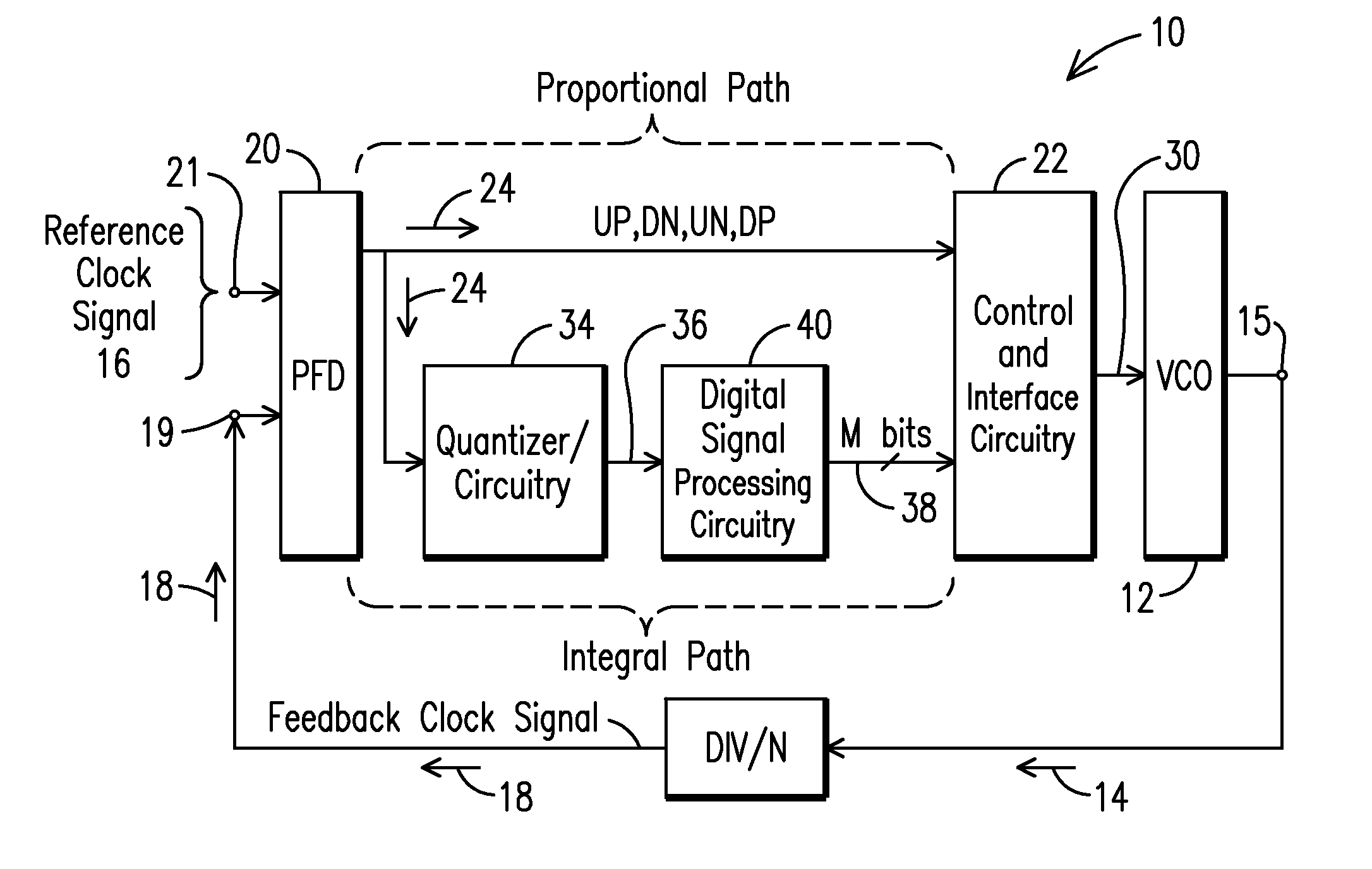
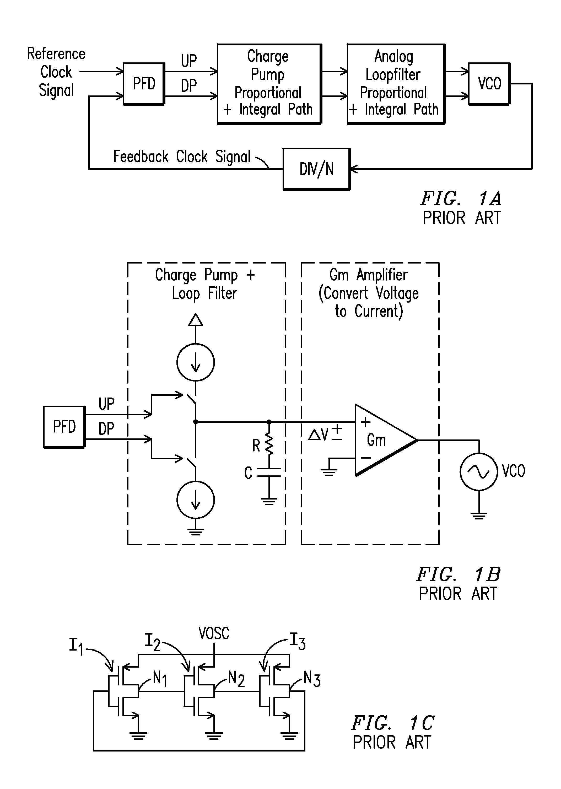
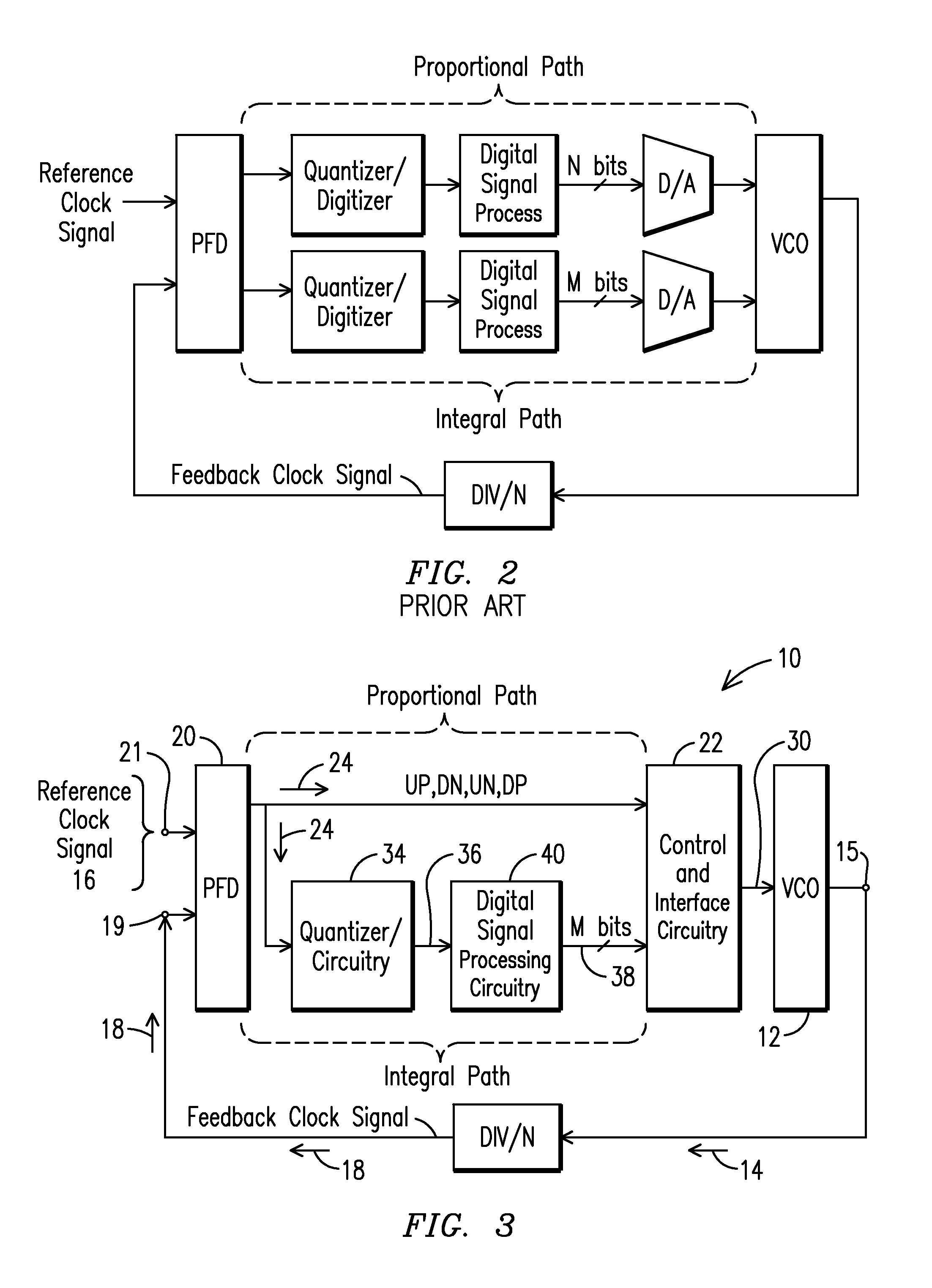
[0033]FIG. 3 illustrates a phase locked loop (PLL) circuit 10 according to an embodiment of the invention. A voltage controlled oscillator (VCO) 12 outputs a signal 14 at a terminal 15 thereof, the phase and frequency of which are adjustable based on a comparison between the signal 14 and a clock reference signal 16. The VCO 12 may be the ring oscillator circuit shown in FIG. 1C. In this example, the desired frequency of the signal 14 is a multiple N of the reference clock signal frequency. To effect phase and frequency control of the VCO 12, a portion of the output signal 14 is factored with divide by N circuitry (DIV / N) 17 to provide a feedback signal 18 as an input to a terminal 19 of a Phase-Frequency Detector (PFD) 20. The reference clock signal 16 is provided as an input to a terminal 21 of the PFD 20.

[0034]Control and interface circuitry 22, positioned between the VCO 12 and the PFD 20, receives inputs both directly and indirectly from the output signal 24 of the PFD 20, whic...


PUM


Abstract

System and method providing multiple circuit paths to control characteristics of periodic signals. In one embodiment first and second detector signals are indicative of a phase and frequency differences between the output signal and a reference signal. A first input signal based on the first detector signal adjusts the phase difference. A first control signal based on the second detector signal has frequency content in high and low frequency ranges. A second input signal based on the control signal reduces the frequency difference. A second control signal based on the second detector signal has relatively low frequency content in the high frequency range. A third input signal based on the second control signal reduces the frequency difference.

Description

PRIORITY BASED ON RELATED APPLICATION[0001]This application claims priority based on U.S. Provisional Application No. 61 / 512,549 filed Jul. 28, 2011.FIELD OF THE INVENTION[0002]The present invention relates to electronic systems and, more specifically, systems which include circuitry that provides multiple circuit paths to control characteristics of periodic signals. In one series of embodiments the invention provides for adjustment of output signals generated by an oscillator such as effected with phase locked loop circuitry.BACKGROUND[0003]The phase locked loop (PLL) circuit is a feedback control circuit which may be analog or digital. A phase detector develops an adjustment signal based on comparison between the output of a local voltage controlled oscillator (VCO) and a reference clock input signal. The adjustment signal is processed to provide a modified input to the VCO which results in a phase or frequency modification to the oscillator output signal. Phase locked loop circui...

Claims


Application Information

Patent Timeline
Patent Type & Authority Applications(United States)
IPC IPC(8): H03L7/08
CPCH03L7/091H03L7/0891
Inventor WANG, ROBERTPIALIS, ANTONIOSMAHADEVAN, RAJEEVANYAGHINI, NAVIDKARAKIEWICS, RAFALTANG, RAYMOND KWOK KEISHEN, SIDAANDRUCHOW, MARKLI, ZHUOBINPANTALEO, NICOLA
Owner INTEL CORP
Why Eureka
Try Eureka