Adhesive die attachment method for a semiconductor die and arrangement for carrying out the method

a technology of adhesive die and semiconductor die, which is applied in the direction of semiconductor devices, electrical equipment, basic electric elements, etc., can solve the problem that partial curing cannot be avoided, and achieve the effects of good mechanical bonding of the die to the substrate, reliable electrical connection, and easy control

Inactive Publication Date: 2005-11-22
BENCH WALK LIGHTING LLC
View PDF8 Cites 6 Cited by
  • Summary
  • Abstract
  • Description
  • Claims
  • Application Information

AI Technical Summary

Benefits of technology

[0012]It is an object of the invention to provide an adhesive die attachment method for attaching a semiconductor die to a substrate, which method does not cause an electrical short to the PN junction of the semiconductor die even if the PN junction is formed very close to the base of the die, which is not particularly sensitive to the amount of adhesive used and, therefore, easy to control, which can be used for any type of dice with different shapes, including such with trapezoid vertical cross-section, and which provides both for a good mechanical bond of the die to the substrate and for a reliable electrical connection between the die and the substrate.
[0013]It is a further object of the invention to provide a suitable, reliable and simple die attaching arrangement to carry out the method according to the invention.
[0015]According to the invention, a small amount of conductive adhesive is deposited onto a substrate. The adhesive deposited is then partially treated by exposing the adhesive to heat, preferably by partial curing and / or drying, so that it becomes partially hardened. In case of partial curing, which happens if the adhesive is subjected to heat, the adhesive is partially polymerized, whereas in case of drying the adhesive the solvent present therein is driven out from the adhesive. According to the invention, the preferable way of pre-treatment of the adhesive is the drying, since this process ensures the necessary hardness of the adhesive and, at the same time, enables the utilization of at least substantially the full polymerization process for the final curing of the adhesive, thereby providing for the strongest possible electrical and mechanical bonding of the die to the substrate. The drying as pre-treatment is carried out by subjecting the adhesive to an elevated (but still low) temperature for a short period of time. However, since every heat treatment of the adhesive brings about also a polymerization of the same, a partial curing can never be avoided, even if primarily a drying is intended.
[0017]As a result of the pressure exerted to the adhesive by the semiconductor die, excess adhesive, if any, is squeezed out from between the die and the substrate. However, as experimented by the inventors of this invention, due to the pre-treatment of the adhesive, the adhesive is squeezed out from between the die and the substrate in such a way that it does not wet up the sides of the die and, accordingly, does not contact the lower region of the semiconductor die to form a fillet around it. Rather, the excess amount of adhesive squeezed out from between the die and the substrate surrounds the lower region of the semiconductor die with a gap between the sides of the die and the squeezed out adhesive. Consequently, the excess adhesive does not cause an electrical short circuit to the PN junction of the semiconductor die. This characteristics of the adhesive attach produced by the adhesive die attaching method according to the invention is particularly advantageous in case of dice with low PN junction, in particular LEDs, laser diodes and photo-detectors.
[0022]According to a preferred embodiment of the invention, the conductive filler used for the adhesive is a metallic or metallic-coated filler. The advantage of such metallic fillers compared to other conductive fillers, like carbon fillers, is that it provides for an excellent conductivity of the adhesive which is necessary in order to achieve a reliable electrical connection between the electrodes provided on the die and the substrate, respectively.

Problems solved by technology

However, since every heat treatment of the adhesive brings about also a polymerization of the same, a partial curing can never be avoided, even if primarily a drying is intended.

Method used


Image

  • Adhesive die attachment method for a semiconductor die and arrangement for carrying out the method
  • Adhesive die attachment method for a semiconductor die and arrangement for carrying out the method
  • Adhesive die attachment method for a semiconductor die and arrangement for carrying out the method

Examples


Embodiment Construction

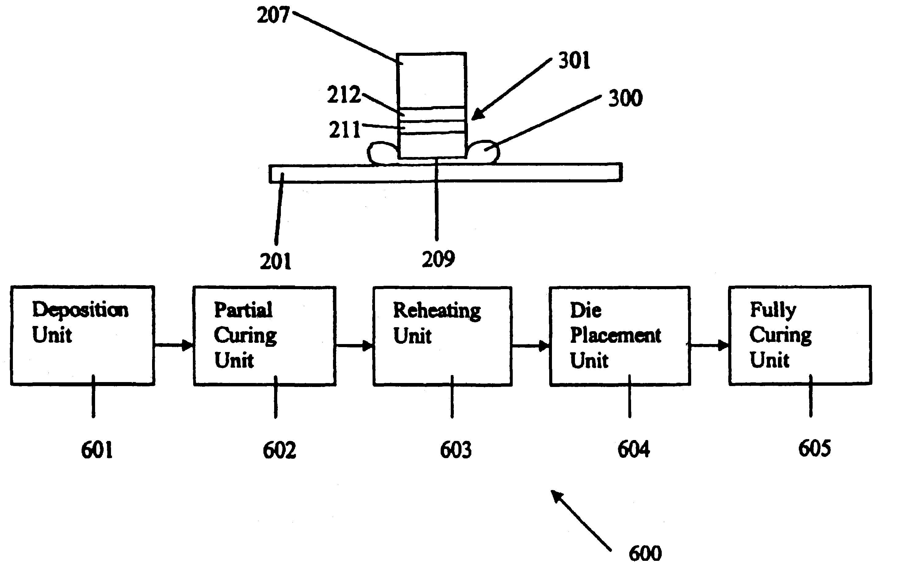
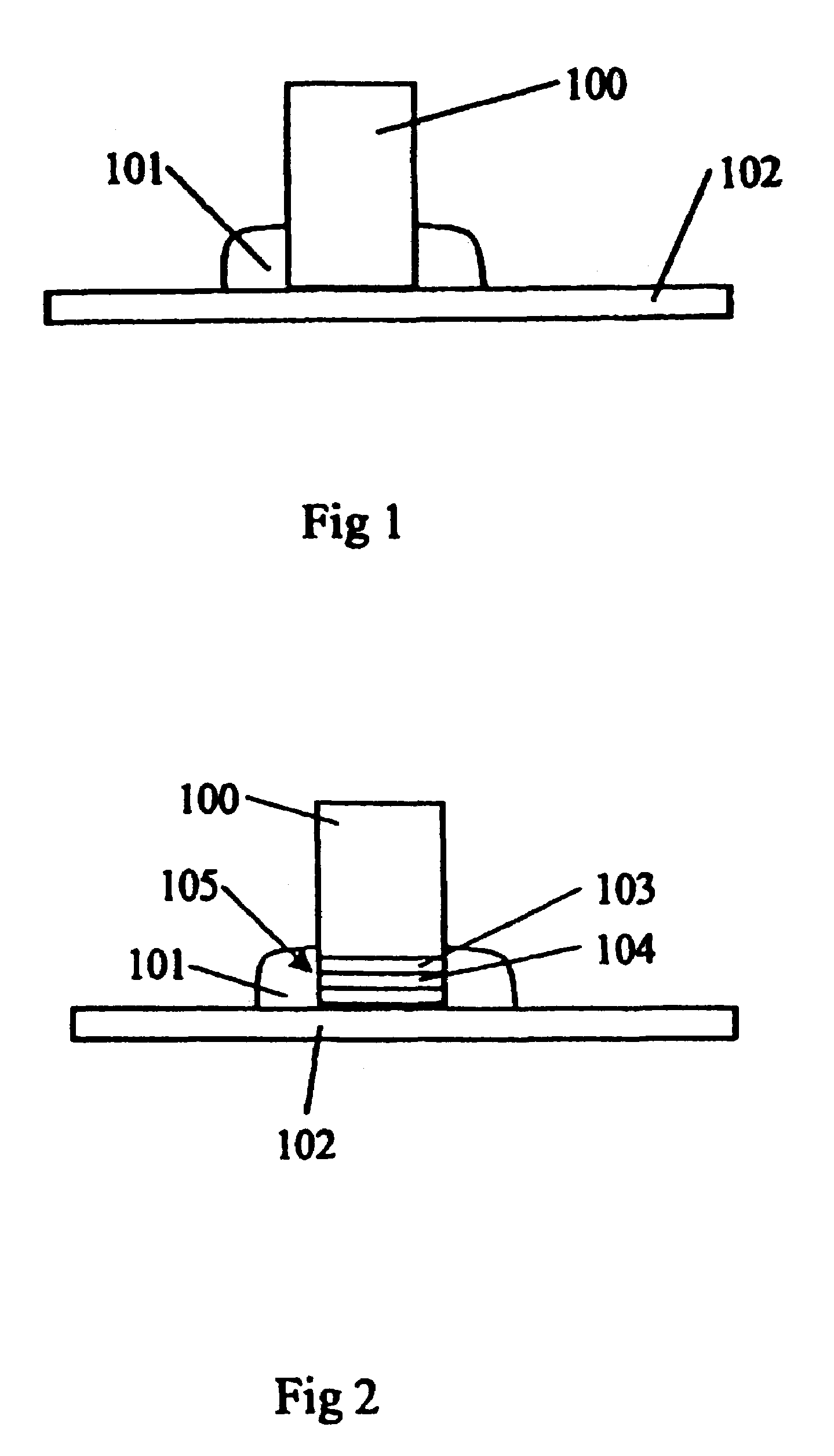
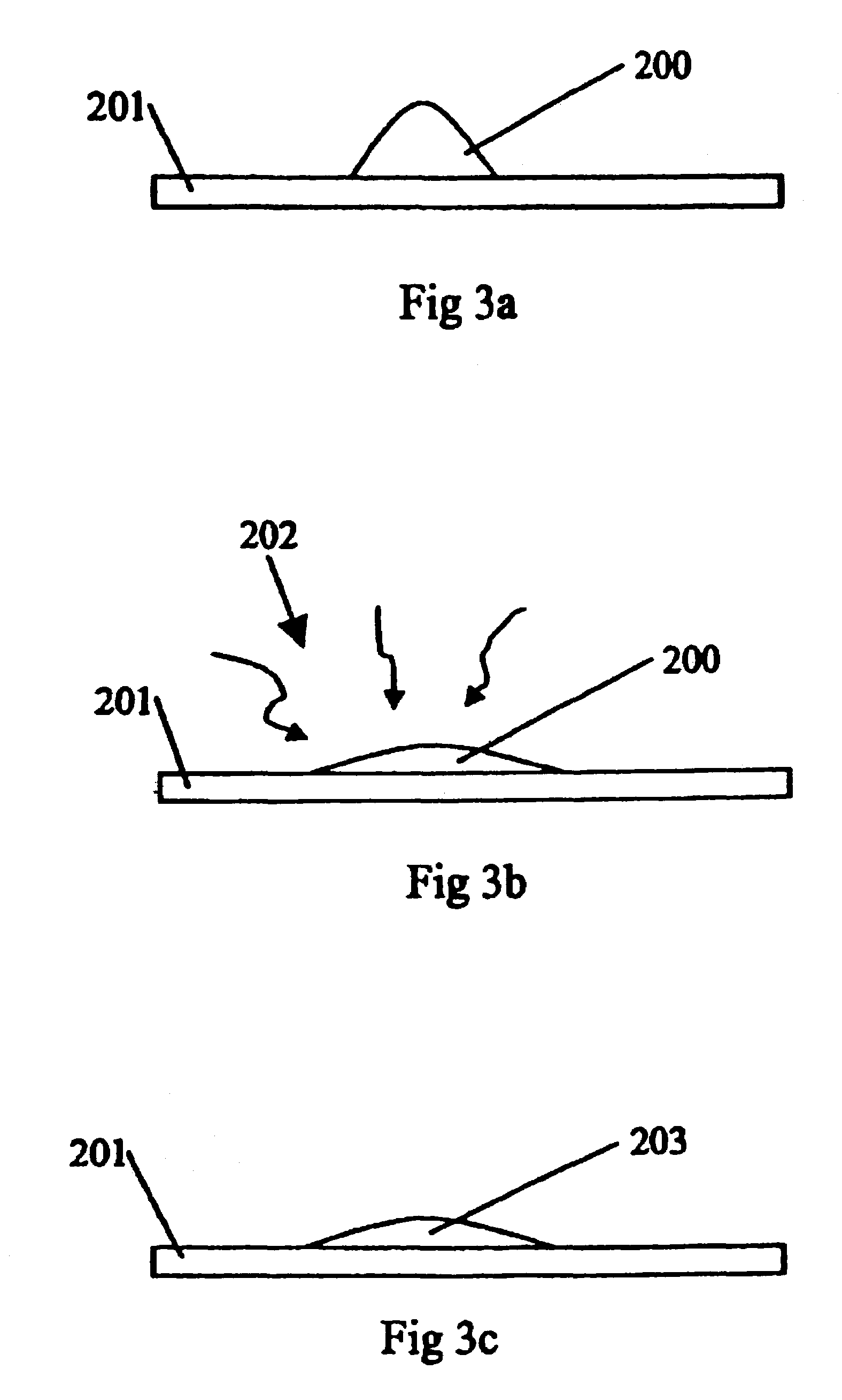
[0040]Preferred embodiments of the adhesive attaching method for attaching a semiconductor die to a substrate according to the invention is shown in, and described in the following with reference to FIG. 3a to FIG. 3h.

[0041]A drop of adhesive 200 is deposited onto a substrate 201 such as a leadframe, a ceramic, glass or flexible circuit board, or a plastic or printed circuit board (PCB), using a dotting, stamping or dispensing process as shown in FIG. 3a. The adhesive may also be deposited on the substrate 201 using a silk-screening, stencilling or ink-jet process.

[0042]According to the preferred embodiment of the invention, the adhesive 200 is formulated from epoxy thermoset resins, thermoplastic resins or silicone. The epoxy is either a one-component or a two-component epoxy formulation consisting of resin as the first component and a catalyst hardener as the second component. The epoxy is also mixed with a metallic filler material to enable the adhesive to be electrically conduc...


PUM


Abstract

The invention relates to an adhesive attaching method for attaching a semiconductor die to a substrate in which an adhesive is deposited onto the substrate, the deposited adhesive is partially cured and / or dried, the partially cured and / or dried adhesive is reheated and a semiconductor die is placed onto the reheated adhesive, after which the adhesive is fully cured so that the semiconductor die is bonded, both electrically and mechanically, to the substrate.

Description

BACKGROUND OF THE INVENTION[0001]This invention relates to a method and a device for attaching a semiconductor die to a substrate in a manner that an electrical short to the PN junction of the semiconductor die is prevented.[0002]Die attaching forms an integral part of a semiconductor chip packaging process. Die attaching or die bonding is the process of mounting a semiconductor die or chip onto a substrate and this process is well established in the field of semiconductor device manufacturing.[0003]One purpose of the die attaching process is to create a strong physical bond between the die and the substrate of the package. However, it also serves to provide either an electrical conducting or insulating contact between the die and the substrate. There are different known die attaching methods, such as eutectic die attachment, soldering die attachment and adhesive die attachment. The choice among the different die attaching methods in a particular case depends on factors like the siz...

Claims


Application Information

Patent Timeline
Patent Type & Authority Patents(United States)
IPC IPC(8): H01L21/58H01L21/02
CPCH01L24/83H01L24/29H01L2224/83192H01L2224/83855H01L2224/83856H01L2924/01005H01L2924/01015H01L2924/01047H01L2924/01075H01L2924/01077H01L2924/01322H01L2924/07802H01L2924/09701H01L2224/2919H01L2924/01006H01L2924/01033H01L2924/014H01L2924/0665H01L2924/00H01L2924/12041H01L2924/12036H01L2924/12042
Inventor NG, KEE YEANSEAH, KEH CHINLEE, CHONG HAI
Owner BENCH WALK LIGHTING LLC
Why Eureka
Try Eureka