Wire structure, a thin film transistor substrate of using the wire structure and a method of manufacturing the same

a thin film transistor and wire structure technology, applied in the field of wire structure, thin film transistor array panel, can solve the problems of low resistance of silver to glass substrate or silicon layer, critical problem of signal distortion due to the increase of the resistance of the wires and in various parasitic capacitances, and achieve the effect of improving reliability and low resistan

Inactive Publication Date: 2005-11-29
SAMSUNG DISPLAY CO LTD
View PDF8 Cites 41 Cited by
  • Summary
  • Abstract
  • Description
  • Claims
  • Application Information

AI Technical Summary

Benefits of technology

[0008]It is another object of the present invention to provide a thin film transistor array panel with a low resistivity Ag wire having improved reliability.

Problems solved by technology

Accordingly, signal distortion due to the increase in the resistance of the wires and in various parasitic capacitances becomes to be a critical problem.
However, silver exhibits poor adhesiveness to a glass substrate or a silicon layer.
The poor adhesivences frequently causes the defect such as the looseness or detachment of the silver thin films during the subsequent processes such as cleaning, which results in the disconnection of the wire.
Furthermore, silver may be easily damaged by dry etch of the silicon nitride insulating layer.

Method used


Image

  • Wire structure, a thin film transistor substrate of using the wire structure and a method of manufacturing the same
  • Wire structure, a thin film transistor substrate of using the wire structure and a method of manufacturing the same
  • Wire structure, a thin film transistor substrate of using the wire structure and a method of manufacturing the same

Examples


first embodiment

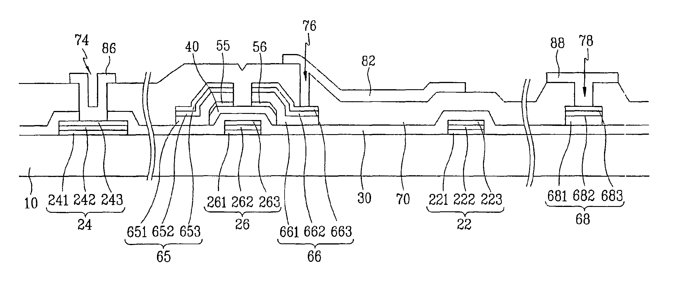
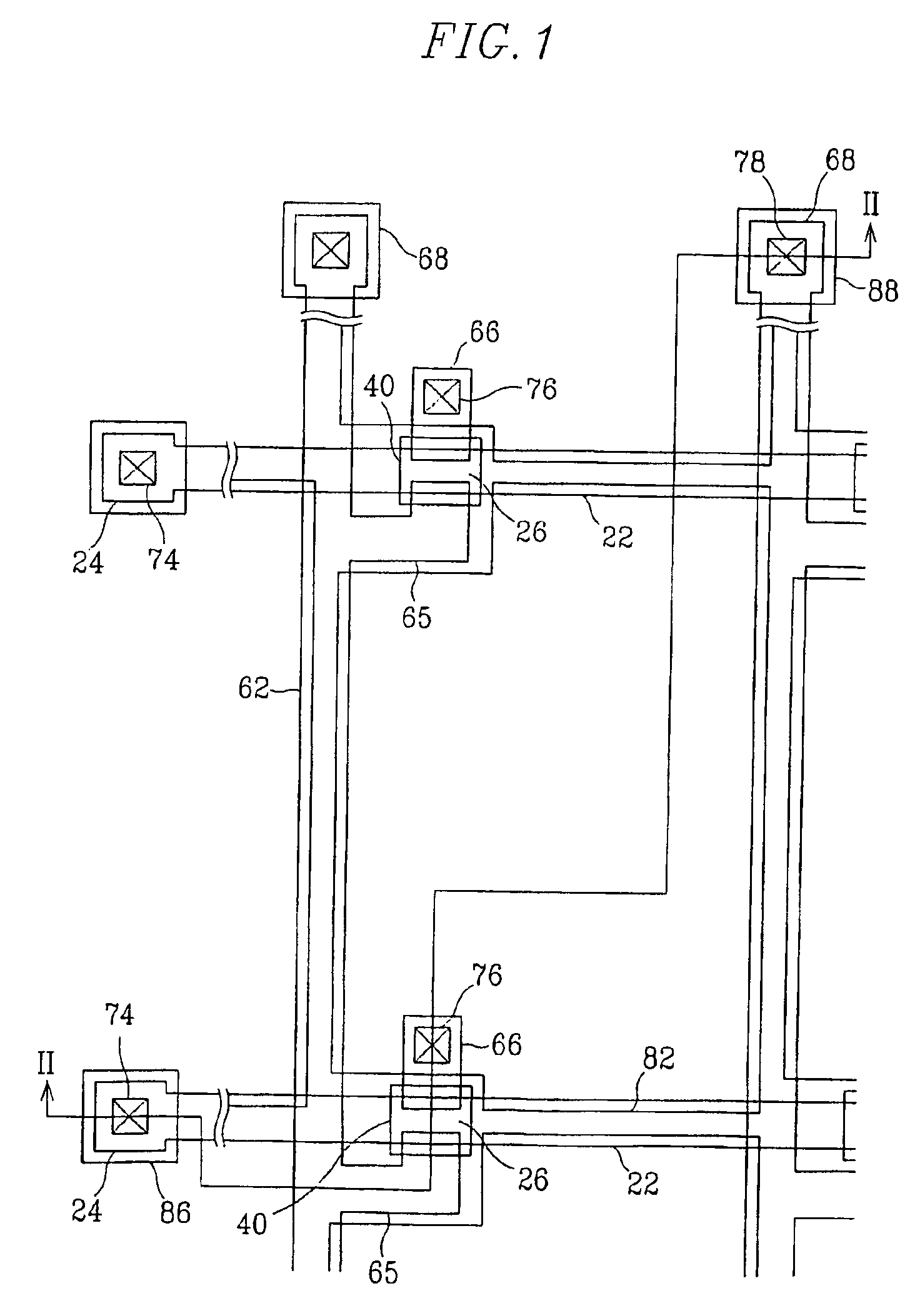
[0063]First, a structure of a TFT array panel for an LCD according to the present invention is described in detail with reference to FIGS. 1 and 2.

[0064]FIG. 1 is a layout view of a TFT array panel for an LCD according to a first embodiment of the present invention, and FIG. 2 is a sectional view of the TFT array panel shown in FIG. 1 taken along the line II—II.

[0065]A gate wire 22, 24 and 26 is formed on an insulating substrate 10. The gate wire 22, 24 and 26 includes triple layers of a first gate layer 221, 241 and 261, a second gate layer 222, 242 and 262 and a third gate layer 223, 243 and 263. The first gate layer 221, 241 and 261 is preferably made of one of Mo, Mo alloy such as MoW, Cr, Cr alloy, Ti, Ti alloy, Ta and Ta alloy. The second gate layer 222, 242 and 262 is preferably made of Ag or Ag alloy, and the third gate layer 223, 243 and 263 is preferably made of indium zinc oxide (“IZO”), Mo or Mo alloy. The first gate layer 221, 241 and 261, which is provided for improvin...

second embodiment

[0088]FIG. 7 is a layout view of a TFT array panel for an LCD according to the present invention, and FIGS. 8 and 9 are sectional views of the TFT array panel shown FIG. 7 taken along the line VIII-VIII′ and the line IX-IX′, respectively.

[0089]A gate wire 22,24 and 26 is formed on an insulating substrate 10. Like the first embodiment, The gate wire 22, 24 and 26 includes triple layers of a first gate layer 221, 241 and 261, a second gate layer 222, 242 and 262 and a third gate layer 223, 243 and 263. The first gate layer 221, 241 and 261 is preferably made of one of Mo, Mo alloy such as MoW, Cr, Cr alloy, Ti, Ti alloy, Ta and Ta alloy. The second gate layer 222, 242 and 262 is preferably made of Ag or Ag alloy, and the third gate layer 223, 243 and 263 is preferably made of indium zinc oxide (“IZO”), Mo or Mo alloy. The first gate layer 221, 241 and 261, which is provided for improving the adhesiveness to the substrate 10, has the thickness of preferably equal to or less than 500 Å....

third embodiment

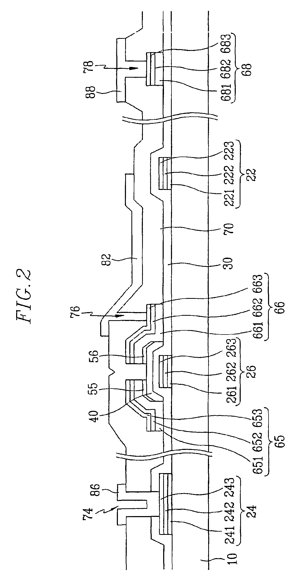
[0137]First, a structure of a TFT array panel for an LCD according to the present invention is described in detail with reference to FIGS. 21 and 22.

[0138]FIG. 21 is a layout view of a TFT array panel for an LCD according to a third embodiment of the present invention, and FIG. 22 is a sectional view of the TFT array panel shown in FIG. 21 taken along the line XXII-XXII′.

[0139]A gate wire 22, 24 and 26 is formed on an insulating substrate 10. The gate wire 22, 24 and 26 includes triple layers of an adhesion layer, a Ag containing layer and a protection layer. The gate wire 22, 24 and 26 includes a plurality of scanning signal lines or gate lines 22 extending in the transverse direction, a plurality of gate pads 24 connected to one ends of the gate lines 22 to transmit gate signals from an external device to the gate lines 22, and a plurality of gate electrodes 26 of TFTs, which are parts of the gate lines 22 to form a plurality of TFTs. The expansions of the gate lines 22 overlap st...


PUM

PropertyMeasurementUnit
dielectric constantaaaaaaaaaa
thicknessaaaaaaaaaa
adhesionaaaaaaaaaa

Abstract

A thin film transistor array panel includes an insulating substrate, a gate wire formed on the insulating substrate. A gate insulating layer covers the gate wire. A semiconductor pattern is formed on the gate insulating layer. A data wire having source electrodes, drain electrodes and data lines is formed on the gate insulating layer and the semiconductor pattern. A protective layer is formed on the data wire. Pixel electrodes connected to the drain electrode via contact holes are formed on the protective layer. The gate wire and the data wire include triple layers of an adhesion layer, a Ag containing layer and a protection layer. The adhesion layer includes one of Cr, Cr alloy, Ti, Ti alloy, Mo, Mo alloy, Ta, Ta alloy, the Ag containing layer includes Ag or Ag alloy, and the protection layer includes one of IZO, Mo, Mo alloy, Cr and Cr alloy.

Description

BACKGROUND OF THE INVENTION[0001](a) Field of the Invention[0002]The present invention relates to a wire structure, a thin film transistor array panel and a manufacturing method thereof.[0003](b) Description of the Related Art[0004]Generally, a thin film transistor array (“TFT”) panel for a liquid crystal display (“LCD”) or an electro-luninescence (“EL”) display is used as a circuit board for driving the respective pixels in an independent manner. The TFT array panel includes a scanning signal wire or a gate wire transmitting scanning signals, an image signal wire or a data wire transmitting image signals, TFTs connected to the gate and the data wire, pixel electrodes connected to the TFTs, a gate insulating layer covering the gate wire for insulation, and a protective layer covering the TFTs and the data wire for insulation. The TFT includes a gate electrode, which is a part of the gate wire, a semiconductor layer forming a channel, source and drain electrodes, which are parts of t...

Claims


Application Information

Patent Timeline
Patent Type & Authority Patents(United States)
IPC IPC(8): G02F1/136G02F1/1343G02F1/1362G02F1/1368G09F9/30H01L21/336H01L21/768H01L29/786H01L51/50H05B33/12
CPCG02F1/136227G02F1/136213G02F2001/13629G02F1/13629G02F1/136
Inventor CHO, BEOM-SEOKJEONG, CHANG-OH
Owner SAMSUNG DISPLAY CO LTD
Why Eureka
Try Eureka