Semiconductor device low temperature test apparatus using electronic cooling element

Inactive Publication Date: 2005-11-29
MONTEREY RES LLC
View PDF3 Cites 11 Cited by
  • Summary
  • Abstract
  • Description
  • Claims
  • Application Information

AI Technical Summary

Benefits of technology

[0015]According to the above aspect of the invention, because the semiconductor device undergoing testing is cooled via the top side and the bottom side thereof by means of electronic cooling elements, the thermostatic chamber is unnecessary and miniaturization of the test apparatus is thus possible. Moreover, the low temperature environment range is minimized to the range of the semiconductor device undergoing testing and temperature control can be performed highly accurately. In addition, it is possible to heat the socket which is on the opposite side from the bottom side of the semiconductor device undergoing testing, by means of the first electronic cooling element, whereby the generation of frost on the socket can be prevented.
[0016]Further,

Problems solved by technology

Ordinarily, operational defects often occur in a high temperature atmosphere, however, for example, in the case of flash memory and the like, a drop in the power source level in a low temperature atmosphere sometimes leads to a defect such that programming operations cannot be performed normally.
There is thus the problem of an increase in size of the test apparatus.
The waiting time required for the temperature drop which corresponds to the accompanying temperature rise induces a decrease in the throughput of the test apparatus.
Furthermore, even after performing this baking process within the thermostatic chamber, when, after the thermostatic chamber has dropped to a low temperature, testing is implemented continually over a long perio

Method used


Image

  • Semiconductor device low temperature test apparatus using electronic cooling element
  • Semiconductor device low temperature test apparatus using electronic cooling element
  • Semiconductor device low temperature test apparatus using electronic cooling element

Examples


Embodiment Construction

[0022]A description of an embodiment of the present invention will be described below referring to the drawings. However, the scope of protection of the present invention is not limited to or by the embodiment below but rather is intended to cover the inventions appearing in the claims as well as any equivalents thereof.

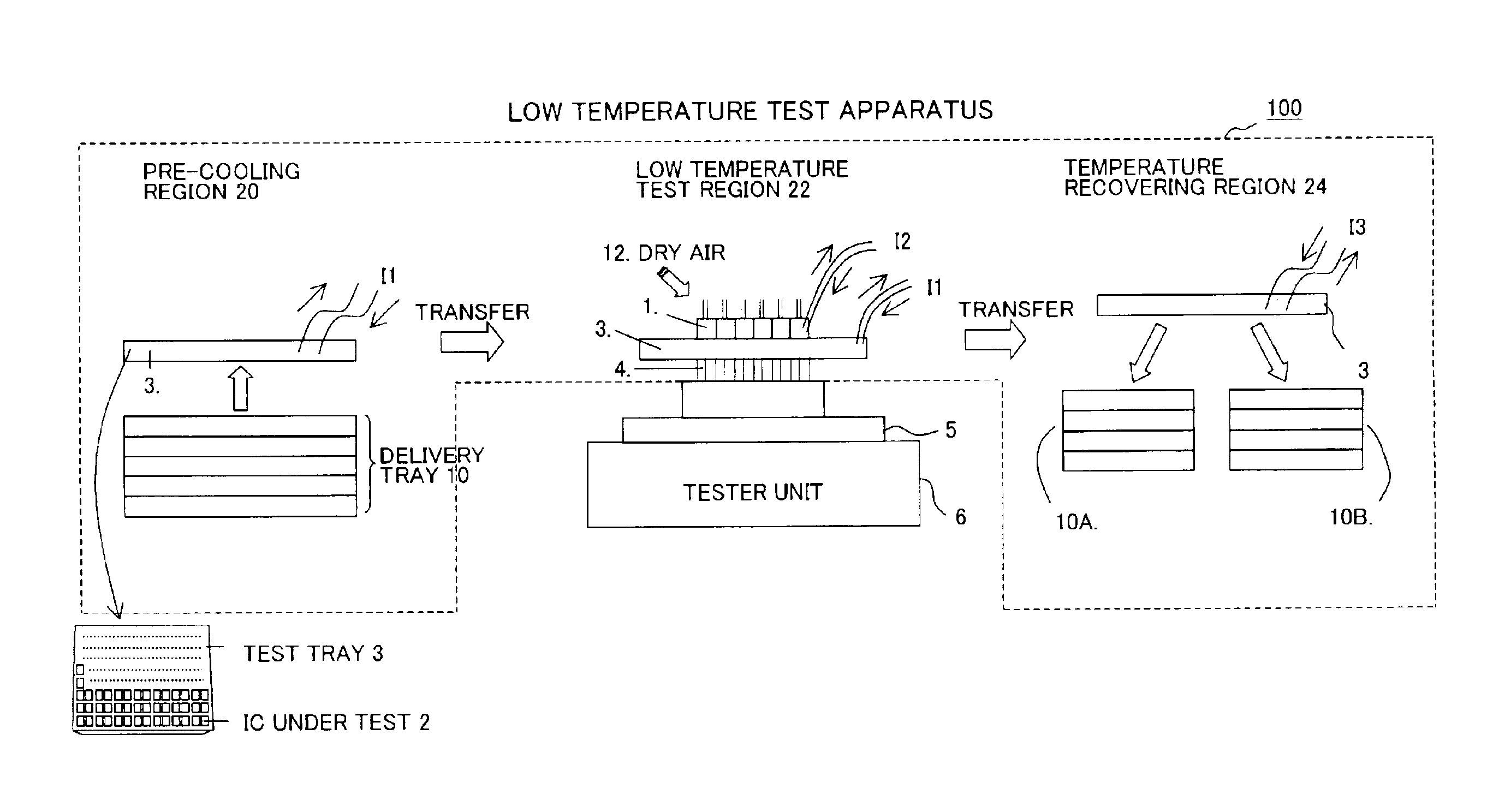
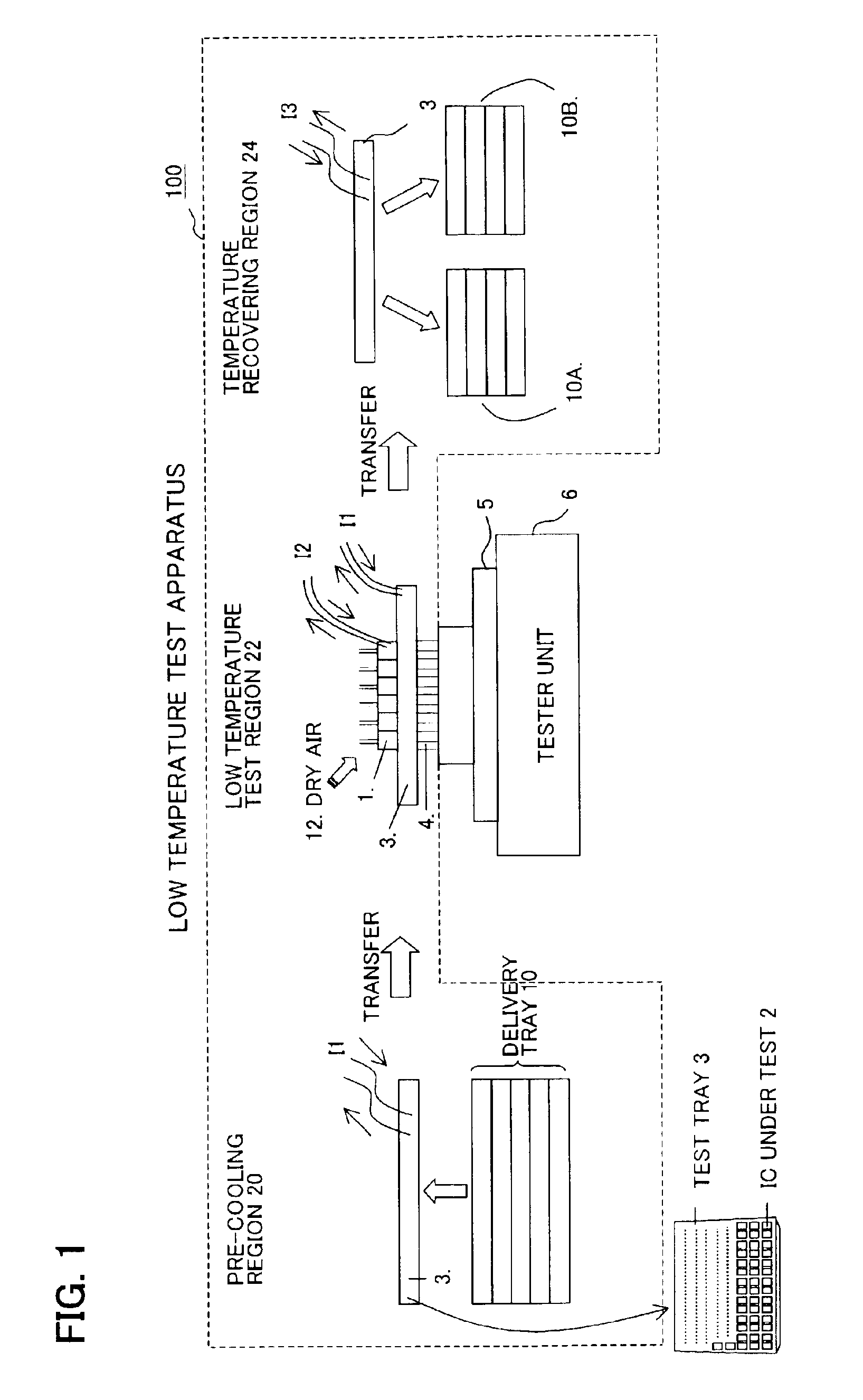
[0023]FIG. 1 is a constitutional view of the low temperature test apparatus according to the present embodiment. This low temperature test apparatus 100 is constituted from a low temperature test region 22 in which a tester unit 6 is connected; a pre-cooling region 20 for pre-cooling an IC undergoing testing; and a temperature recovery region 24 for restoring the IC undergoing testing to a normal temperature after the test is complete. In the low temperature test region 22, the tester unit 6 is connected, the tester unit 6 being provided with a measurement board 5, and a measurement IC socket 4, which is connected to the measurement board 5, is provided.
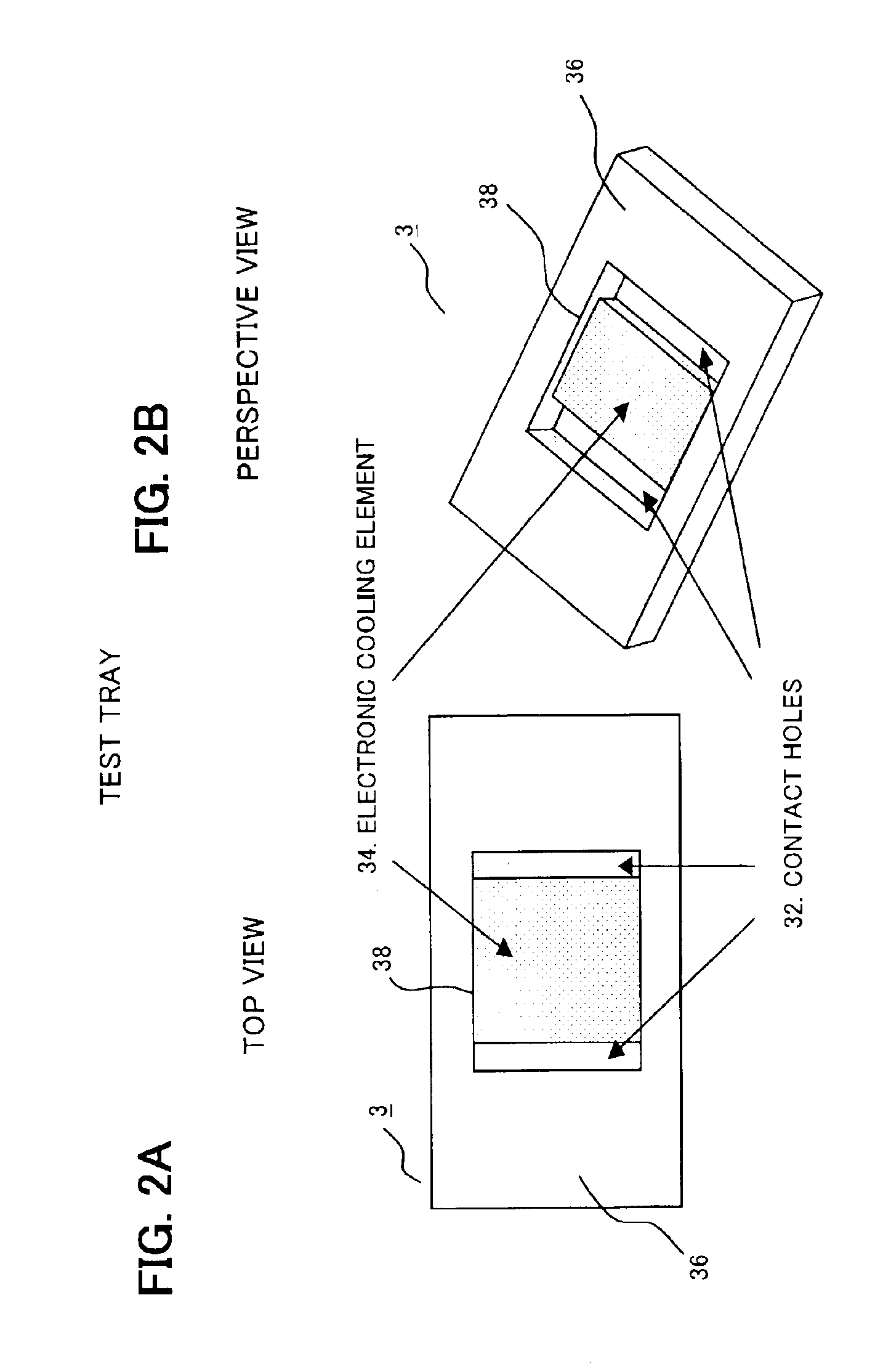
[0024]A deliv...


PUM


Abstract

A semiconductor device test apparatus, has: a socket, which connects to a semiconductor device undergoing testing mounted thereon; a test tray, which houses the semiconductor device undergoing testing and which is provided, in a position on which the semiconductor device undergoing testing is mounted, with a first electronic cooling element that absorbs heat via one surface thereof and releases heat via the other surface thereof; and a contact block, which is provided with a second electronic cooling element that makes contact with the top of the semiconductor device undergoing testing in a state in which the semiconductor device undergoing testing is mounted on the socket.

Description

CROSS-REFERENCE TO RELATED APPLICATIONS[0001]This application is based upon and claims the benefit of priority from the prior Japanese Patent Application No. 2002-120548, filed on Apr. 23, 2002, the entire contents of which are incorporated herein by reference.BACKGROUND OF THE INVENTION[0002]1. Field of the Invention[0003]The present invention relates to a semiconductor device low temperature test apparatus, and more particularly to a low temperature test apparatus that prevents a drop in measurement quality resulting from the generation of frost, dispenses with the conventional thermostatic chamber to thereby miniaturize the apparatus, and shortens the turnaround time.[0004]2. Description of the Related Art[0005]A shipping test for a semiconductor integrated circuit device such as an LSI (referred to as an IC hereinbelow) includes a high temperature test step and a low temperature test step. Generally, the operation of the IC is ensured over a comparatively broad temperature range...

Claims


Application Information

Patent Timeline
IPC IPC(8): G01R31/26G01R31/28
CPCG01R31/2875
Inventor MIYAKITA, SHIGERU
Owner MONTEREY RES LLC
Why Eureka
Try Eureka