Atomic layer deposition (ALD) high permeability layered magnetic films to reduce noise in high speed interconnection

a magnetic film, high-permeability technology, applied in the direction of line-transmission details, waveguide type devices, waveguides, etc., can solve the problems of difficult to achieve larger values, limited switching time in cmos circuits, and general slow switching time response or signal delay of voltage signaling, so as to improve the signal-to-noise ratio and minimize the mutual inductance between neighboring transmission lines

Inactive Publication Date: 2005-11-29
MICRON TECH INC
View PDF96 Cites 59 Cited by
  • Summary
  • Abstract
  • Description
  • Claims
  • Application Information

AI Technical Summary

Benefits of technology

[0011]The at least one shield structure formed by ALD at least partially shields neighboring transmission lines from the magnetic fields generated around the respective transmission lines when they transmit an electrical signal. Thereby, mutual inductance between neighboring transmission lines is minimized and the signal to noise ratio is improved.

Problems solved by technology

Most commonly used coaxial lines have an impedance of 50 ohms or 75 ohms, as it is difficult to achieve larger values.
Switching times in CMOS circuits have been limited by the ability to switch the capacitive loads of long lines and buffers, and charge these capacitances over large voltage swings to yield a voltage step signal.
The switching time response or signal delay where voltage signaling is used is generally slow if the transmission line is long.
Further, if two transmission lines are in close proximity to one another, the voltage swing on one line can induce a large voltage swing or noise voltage on a neighboring transmission line.
In a system utilizing signal currents over low impedance transmission lines, the noise current will be a few percent of the signal current and the noise to signal ratio will become undesirable.

Method used


Image

  • Atomic layer deposition (ALD) high permeability layered magnetic films to reduce noise in high speed interconnection
  • Atomic layer deposition (ALD) high permeability layered magnetic films to reduce noise in high speed interconnection
  • Atomic layer deposition (ALD) high permeability layered magnetic films to reduce noise in high speed interconnection

Examples


fifth embodiment

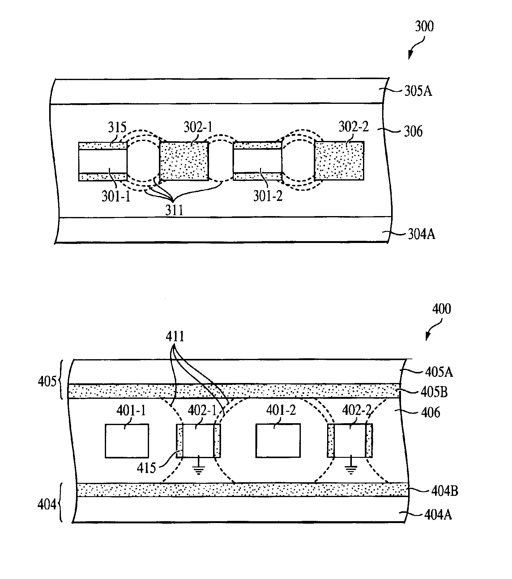
[0106]FIG. 6A illustrates neighboring transmission lines in accordance with the invention. A number of transmission lines 601-1, 601-2 are spaced between a number of electrically conductive lines 602-1, 602-2, which are shown grounded. For simplicity, a pair of transmission lines 601-1, 601-2 and a pair of electrically conductive lines 602-1, 602-2 are shown, but the invention has applicability to any number of transmission lines spaced between any number of electrically conductive lines. Preferably, the transmission lines 601-1, 601-2 and the electrically conductive lines 602-1, 602-2 are spaced parallel to one another.

[0107]The transmission lines 601-1, 601-2 are spaced between a conductive plane 604A and a sandwich layer 605. Further, in this embodiment, the transmission lines 601-1, 601-2 include shield layers 615 formed on a number of surfaces thereon. Preferably, shield layers 615 are formed on three surfaces of the transmission lines 601-1, 601-2, including opposing sides adj...

sixth embodiment

[0113]FIG. 7 illustrates neighboring transmission lines in accordance with the invention. A number of transmission lines 701-1, 701-2 are spaced between a number of electrically conductive lines 702-1, 702-2, which are grounded. For simplicity, a pair of transmission lines 701-1, 701-2 and a pair of electrically conductive lines 702-1, 702-2 are shown, but the invention has applicability to any number of transmission lines spaced between any number of electrically conductive lines. Preferably, the transmission lines 701-1, 701-2 and the electrically conductive lines 702-1, 702-2 are spaced parallel to one another.

[0114]The transmission lines 701-1, 701-2 are spaced between sandwich layers 704 and 705. Further, in this embodiment, the electrically conductive lines 702-1, 702-2 include shield layers 715 formed on a number of surfaces thereof. Preferably, shield layers 715 are formed on three surfaces of the electrically conductive lines 702-1, 702-2, including opposing sides adjacent ...


PUM


Abstract

A structure for magnetically shielded transmission lines for use with high speed integrated circuits having an improved signal to noise ratio, and a method for forming the same are disclosed. At least one magnetic shield structure formed by atomic layer deposition (ALD) contains electrically induced magnetic fields generated around a number of transmission lines. The shield material is made of alternating layers of magnetic material and insulating material.

Description

FIELD OF THE INVENTION[0001]The present invention relates to the field of integrated circuits, and in particular to improved transmission lines for high speed interconnections.BACKGROUND OF THE INVENTION[0002]The metal lines over insulators and ground planes, metal lines buried in close proximity to dielectric insulators and used for integrated circuit interconnects, and interconnection lines on interposers and printed circuit boards are in reality transmission lines. The use of coaxial interconnections through the substrate in CMOS integrated circuits can also be considered transmission lines.[0003]The low characteristic impedance of these interconnection lines results in part from the low characteristic impedance of free space, Z0=(μ0 / ε0)1 / 2=377 ohms, and in part from the dielectric material used for electrical insulation in the lines which has a higher dielectric permittivity than free space. Most commonly used coaxial lines have an impedance of 50 ohms or 75 ohms, as it is diffi...

Claims


Application Information

Patent Timeline
Patent Type & Authority Patents(United States)
IPC IPC(8): H01L23/522H01L23/552H05K1/02
CPCH01L23/5225H01L23/552H05K1/0233H01L2924/3011H05K1/0219H05K2201/083H05K2201/09236H01L2924/0002H01L2924/00
Inventor AKRAM, SALMANAHN, KIE Y.FORBES, LEONARD
Owner MICRON TECH INC
Why Eureka
Try Eureka