Semiconductor laser device, fabricating method thereof and optical pickup employing the semiconductor laser device

a laser device and semiconductor technology, applied in semiconductor lasers, optical pickups, optical beam sources, etc., can solve the problems of high material cost of metal brazing materials, high material cost of side beams reflecting on chip surfaces, stem surfaces, etc., and achieve the effect of reducing the time of die bonding process, reducing the occupation time of the bonding place, and reducing the cost of material costs

Inactive Publication Date: 2005-12-06
SHARP KK
View PDF18 Cites 2 Cited by
  • Summary
  • Abstract
  • Description
  • Claims
  • Application Information

AI Technical Summary

Benefits of technology

[0031]Furthermore, by employing the conductive die bonding paste as the die bonding adhesive of the semiconductor laser chip, the material cost is less expensive than that of the metal brazing material or the like. In addition, the heating and curing of the conductive die bonding paste is allowed to be performed after the die bonding, meaning that neither heating nor cooling in the place or apparatus of die bonding is required. This enables the reduction in time of the die bonding process and the reduction in the occupation time of the bonding place (apparatus). As a result, an inexpensive high-reliability high-productivity semiconductor laser device and a fabricating method thereof can be obtained.

Problems solved by technology

From this standpoint, the conventional semiconductor laser devices have had the problems that much time is necessary for the heating and cooling cycles of the metal brazing material (gold-tin alloy solder or a low-melting-point brazing material In) and that the material cost of the metal brazing material is high.
However, according to an optical pickup and, in particular, an optical pickup that employs a 3-beam system, return light of side beams reflecting on the chip surface, stem surface and the like of the optical pickup, exerts a bad influence.

Method used


Image

  • Semiconductor laser device, fabricating method thereof and optical pickup employing the semiconductor laser device
  • Semiconductor laser device, fabricating method thereof and optical pickup employing the semiconductor laser device
  • Semiconductor laser device, fabricating method thereof and optical pickup employing the semiconductor laser device

Examples


first embodiment

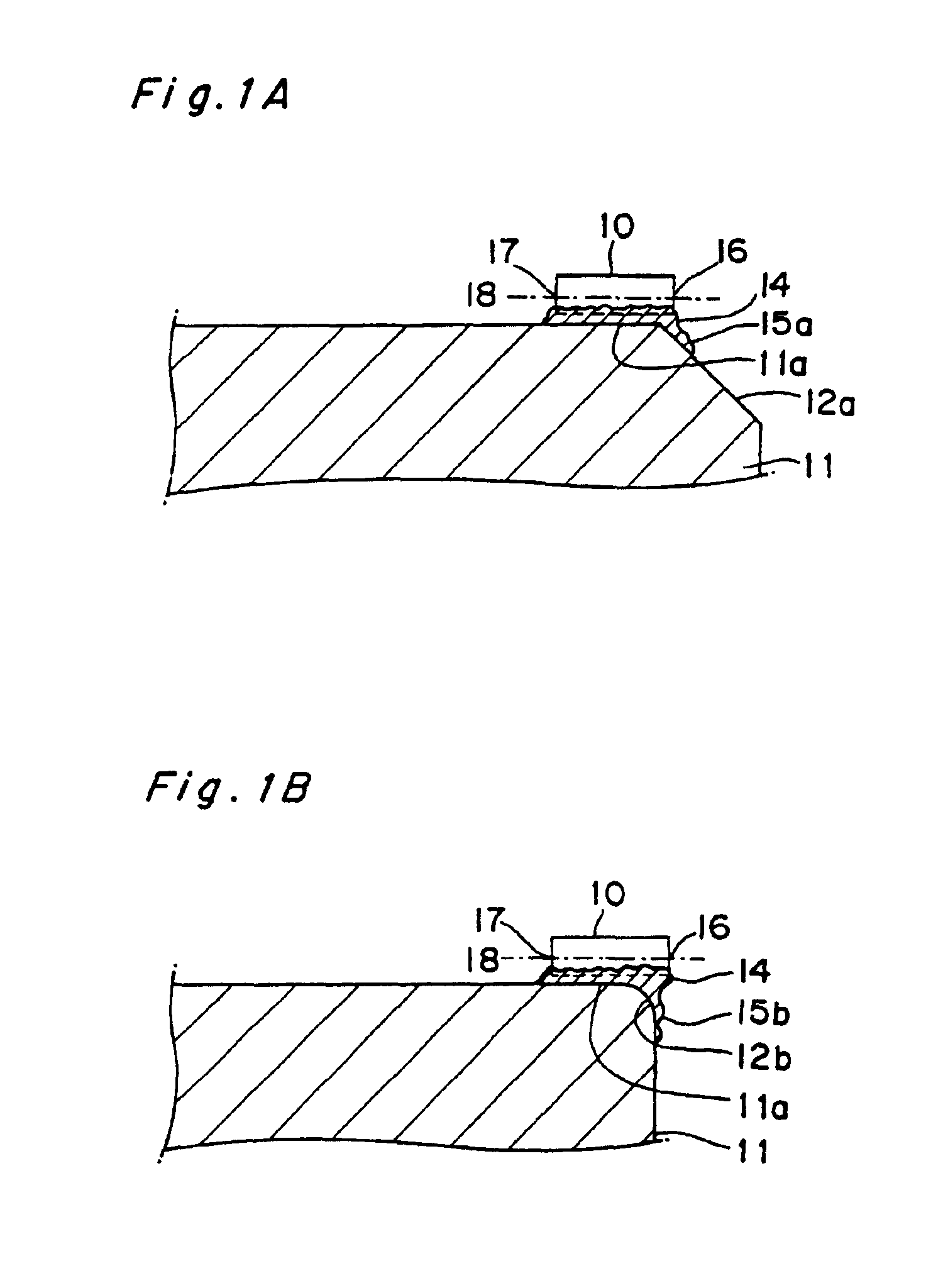
[0044]In FIG. 1A are shown a semiconductor laser chip 10, a stem 11, a header portion 11a of the stem, a chamfered portion 12a provided for the header portion located at an end of the stem, a conductive die bonding paste 14, a conductive die bonding paste 15a flowed onto the chamfered portion 12a, a main radiation side light emission point 16, a monitor side light emission point 17 and an emission light optical axis 18 that connects the main radiation side light emission point with the monitor side light emission point.

[0045]In FIG. 1B are shown a rounded corner portion 12b provided for the header portion located at an end of the stem and a conductive die bonding paste 15b flowed onto the rounded corner portion 12b. The other constituent elements are identical to those of FIG. 1A, and therefore, no description is provided for them.

[0046]Referring to FIGS. 1A and 1B, the stem 11 of the semiconductor laser device is formed by processing a parent material made of an iron-based or coppe...

second embodiment

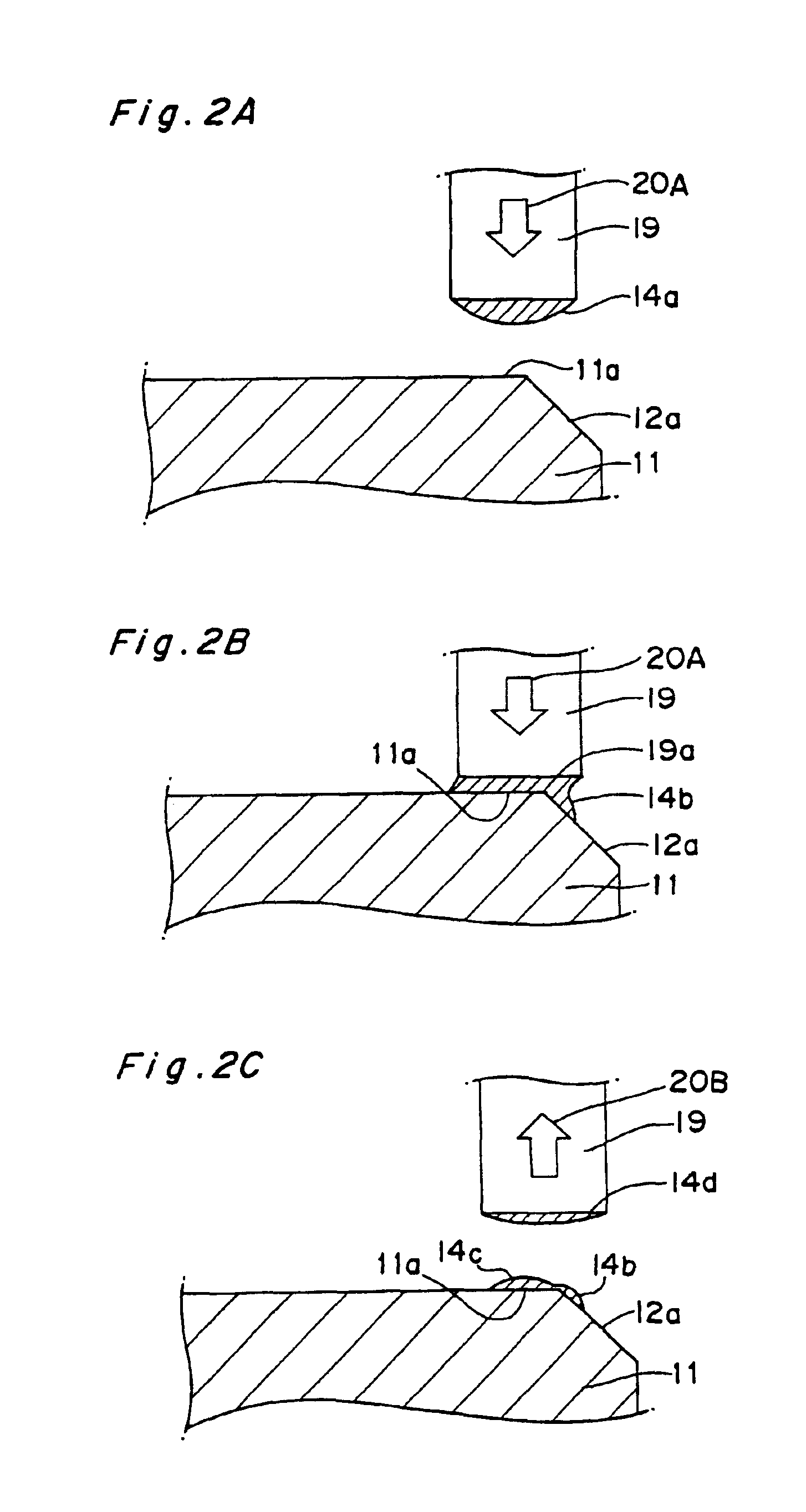
[0068]FIG. 3 shows a semiconductor laser device according to the second embodiment of the present invention, while FIGS. 4A and 4B show the die bonding process of the fabricating method of the device.

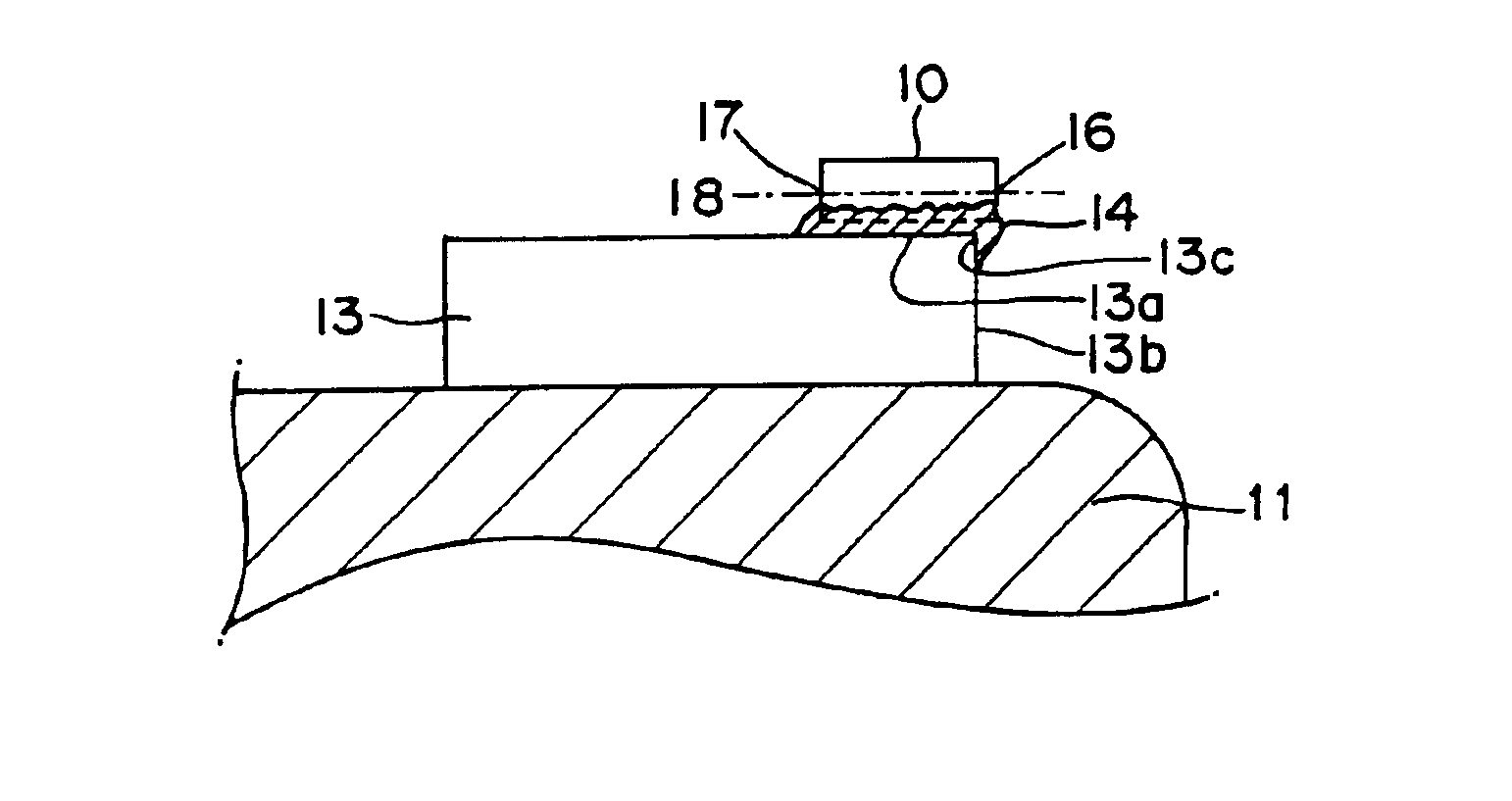
[0069]In FIG. 3 are shown a semiconductor laser chip 10, a stem 11, a header portion 11a of the stem 11, a sub-mount 13, a header portion 13a of the sub-mount, an end surface 13b of the sub-mount, a corner portion i.e. an edge portion 13c of the header portion 13a, a conductive die bonding paste 14, a main radiation side light emission point 16, a monitor side light emission point 17 and a semiconductor laser device emission light optical axis 18 that connects the main radiation side light emission point with the monitor side light emission point. The sub-mount 13 is formed of an Si-based wafer or a ceramic-based material of AlN, SiC or the like and is provided with an electrode pattern or a photodiode as the need arises. The sub-mount 13 is stuck and fixed in a specified position on th...

third embodiment

[0082]FIG. 5 shows an optical pickup according to the third embodiment of the present invention. The optical pickup of the present invention employs the semiconductor laser device of the present invention and includes at least the semiconductor laser device of the present invention, a diffraction grating and a photodetector.

[0083]Referring to FIG. 5, an optical pickup 100 of the present invention is constructed of the semiconductor laser device 101 of the present invention, which has been described in connection with the aforementioned first embodiment or the second embodiment, a diffraction grating 102, a beam splitter 103, a photodetector 104, a collimator lens (condenser lens) 105 and an object lens 106 provided with an actuator.

[0084]Laser light 109 emitted from the main radiation side light emission point 108 of the semiconductor laser chip 107 of the semiconductor laser device 101 is split by the diffraction grating 102 into 3-beam light comprised of zero-order light L0 (main ...


PUM

PropertyMeasurementUnit
temperatureaaaaaaaaaa
heightaaaaaaaaaa
diameteraaaaaaaaaa

Abstract

In a semiconductor laser device, a semiconductor laser chip is placed on a stem so that an end surface of the semiconductor laser chip, on which the main radiation side light emission point is located, protrudes from an edge of a header portion of the stem or from an edge of a header portion of a sub-mount provided on the stem so as to conceal no light emission points of the semiconductor. A conductive die bonding paste is used for the die bonding of the semiconductor laser chip. A chamfered portion or a rounded corner portion is formed at the edge of the header portion of the stem or the edge of the header portion of the sub-mount provided on the stem. Also, an optical pickup is constructed of at least the semiconductor laser device, a diffraction grating, a photodetector, a condenser lens and an object lens.

Description

[0001]This application is a divisional of application Ser. No. 09 / 725,513 filed Nov. 30, 2000 now U.S. Pat. No. 6,700,911, the disclosure of which is hereby incorporated herein by reference.BACKGROUND OF THE INVENTION[0002]The present invention relates to semiconductor laser devices, and in particular, to a semiconductor laser chip mounting structure and fabricating method and an optical pickup employing the device.[0003]Prior art semiconductor laser devices are shown in FIG. 6 through FIG. 9, and the die bonding process of one prior art semiconductor laser device fabricating method is shown in FIGS. 10A and 10B.[0004]In the prior art semiconductor laser device of FIG. 6, a semiconductor laser chip 50 is placed in a specified position of a header portion 51a located at an end of a stem 51 via a metal brazing material (solder or the like) 52. The semiconductor laser chip 50 is bonded by the metal brazing material 52 in the place where the chip is to be die-bonded. Therefore, in the b...

Claims


Application Information

Patent Timeline
Patent Type & Authority Patents(United States)
IPC IPC(8): G11B7/135G11B7/125G11B7/22H01S5/02H01S5/0233H01S5/02375H01S5/30
CPCH01S5/0226H01S5/02268H01S5/005H01S5/02236H01S2301/02H01S5/0236H01S5/02375H01S5/023H01S5/0233H01S5/0235H01S5/30
Inventor KOHASHI, IKUOHAMAOKA, OSAMUHORIGUCHI, TAKESHI
Owner SHARP KK
Why Eureka
Try Eureka