Manufacturing a conformal atomic liner layer in an integrated circuit interconnect
- Summary
- Abstract
- Description
- Claims
- Application Information
AI Technical Summary
Benefits of technology
Problems solved by technology
Method used
Image

Examples
Embodiment Construction
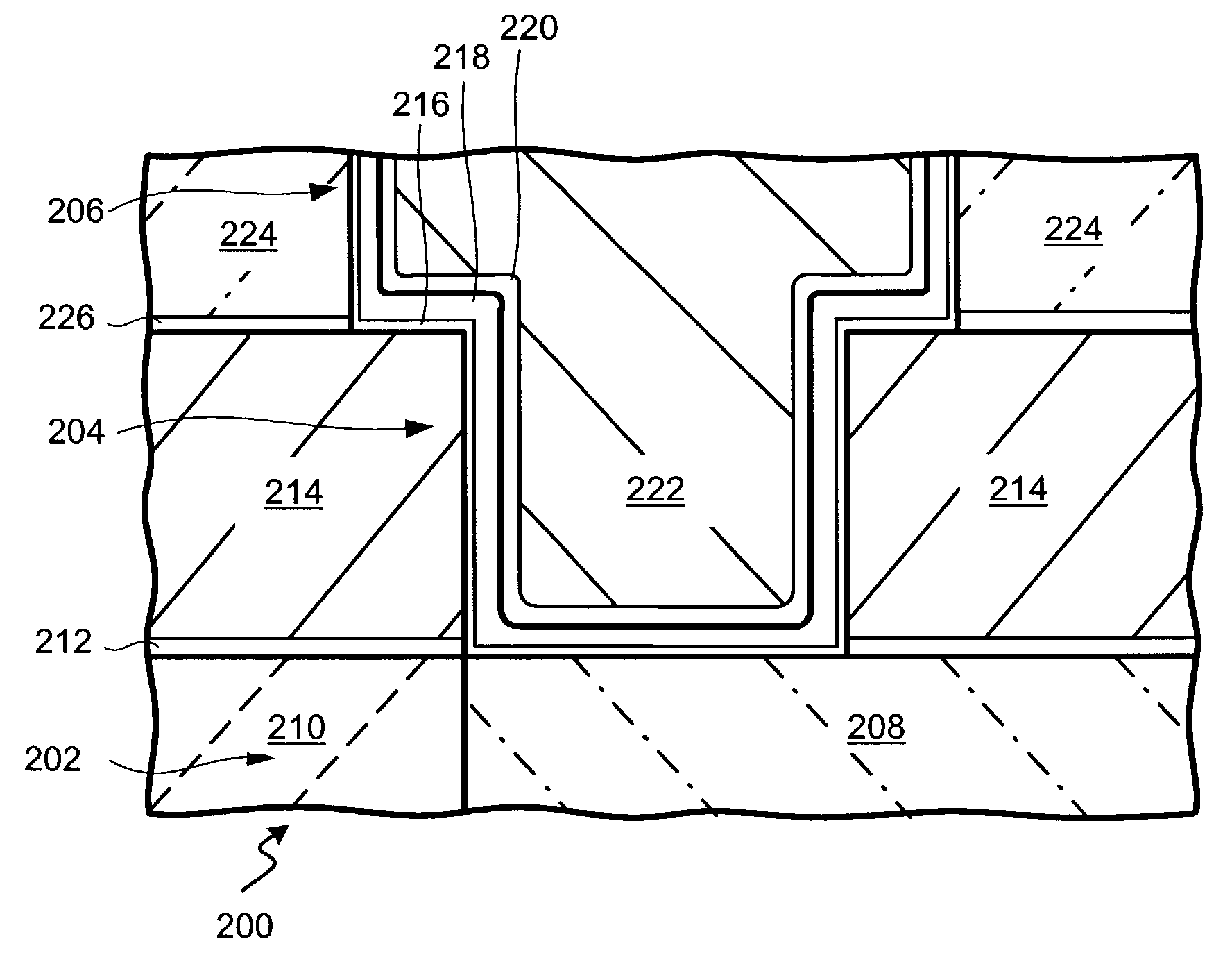
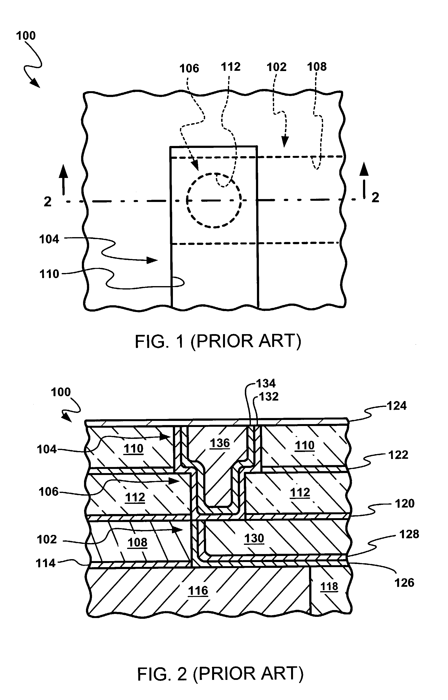
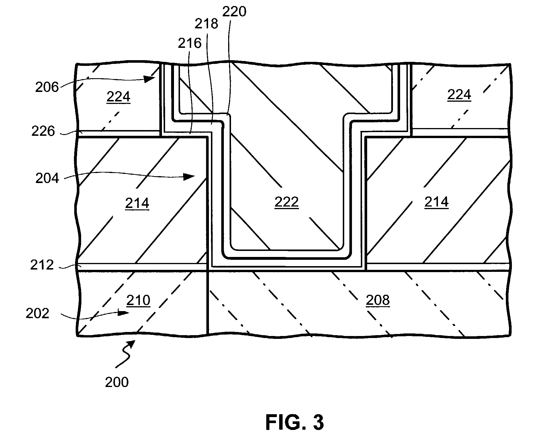
[0035]Referring now to FIG. 1 (PRIOR ART), therein is shown a plan view of a semiconductor wafer 100 with a silicon semiconductor substrate (not shown) having as interconnects first and second channels 102 and 104 connected by a via 106. The first and second channels 102 and 104 are respectively disposed in first and second channel dielectric layers 108 and 110. The via 106 is an integral part of the second channel 104 and is disposed in a via dielectric layer 112.
[0036]The term “horizontal” as used in herein is defined as a plane parallel to the conventional plane or surface of a wafer, such as the semiconductor wafer 100, regardless of the orientation of the wafer. The term “vertical” refers to a direction perpendicular to the horizontal as just defined. Terms, such as “on”, “above”, “below”, “side” (as in “sidewall”), “higher”, “lower”, “over”, and “under”, are defined with respect to the horizontal plane.
[0037]Referring now to FIG. 2 (PRIOR ART), therein is shown a cross-section...
PUM
 Abstract
Description
Claims
Application Information
 - Generate Ideas
- Intellectual Property
- Life Sciences
- Materials
- Tech Scout
- Unparalleled Data Quality
- Higher Quality Content
- 60% Fewer Hallucinations
Browse by: Latest US Patents, China's latest patents, Technical Efficacy Thesaurus, Application Domain, Technology Topic, Popular Technical Reports.
© 2025 PatSnap. All rights reserved.Legal|Privacy policy|Modern Slavery Act Transparency Statement|Sitemap|About US| Contact US: help@patsnap.com