Sub-ranging pipelined charge-domain analog-to-digital converter with improved resolution and reduced power consumption

Inactive Publication Date: 2005-12-06
MASSACHUSETTS INST OF TECH
View PDF16 Cites 19 Cited by
  • Summary
  • Abstract
  • Description
  • Claims
  • Application Information

AI Technical Summary

Benefits of technology

[0009]A pipelined analog-to-digital converter in which signal value samples are represented differentially by pairs of charges and which uses charge-coupled-devices (CCDs) for storage, transport, and arithmetic operations on the charges is presented. In the pipeline, each successive stage resolves an equal or smaller charge difference.

Problems solved by technology

That is, each of these architectures has strengths and weaknesses that make them more amenable to working in certain frequency and resolution ranges.
Flash ADCs, for example, provide the highest available sampling rates, but at relatively limited resolution and at relatively high power consumption.
At the other extreme, sigma-delta ADCs provide very high resolution, but relatively low output sampling rate.
The op-amps limit circuit speed and consume considerable power.
A principal reason for this limit is the difficulty of precisely and non-destructively comparing charges in CCD shift registers.
This floating

Method used


Image

  • Sub-ranging pipelined charge-domain analog-to-digital converter with improved resolution and reduced power consumption
  • Sub-ranging pipelined charge-domain analog-to-digital converter with improved resolution and reduced power consumption
  • Sub-ranging pipelined charge-domain analog-to-digital converter with improved resolution and reduced power consumption

Examples


Embodiment Construction

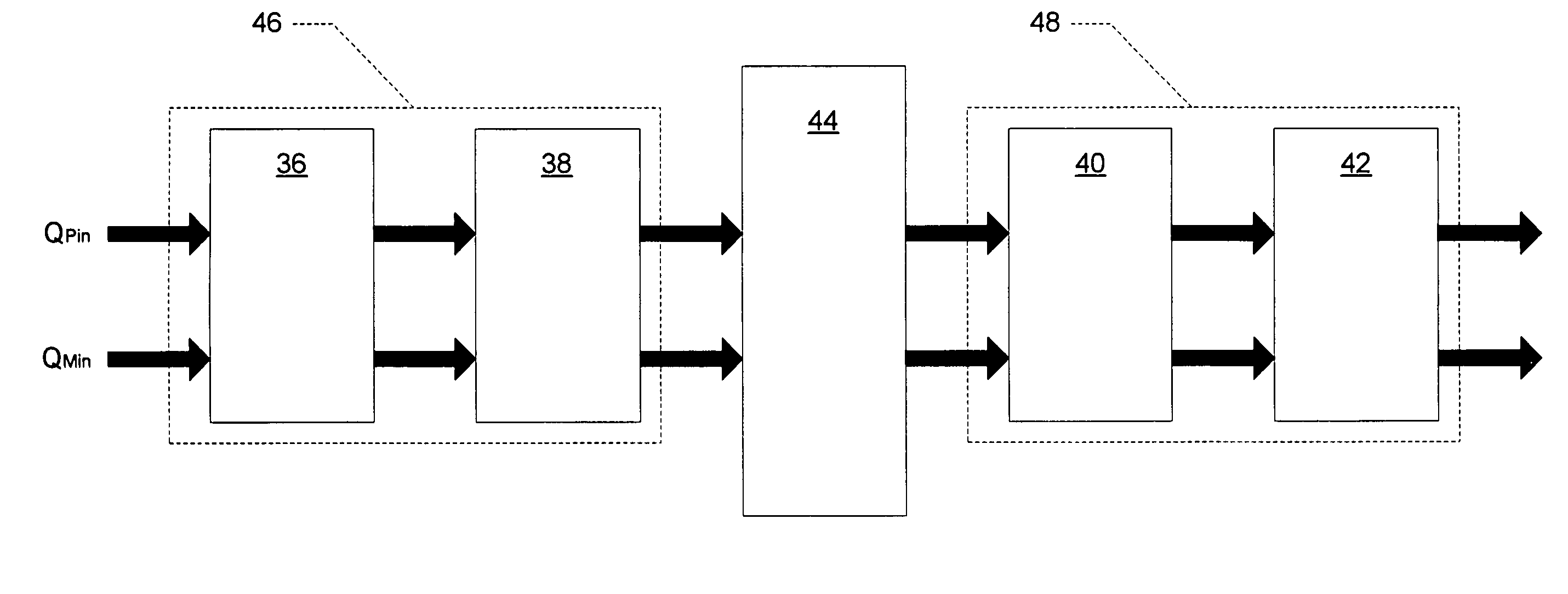
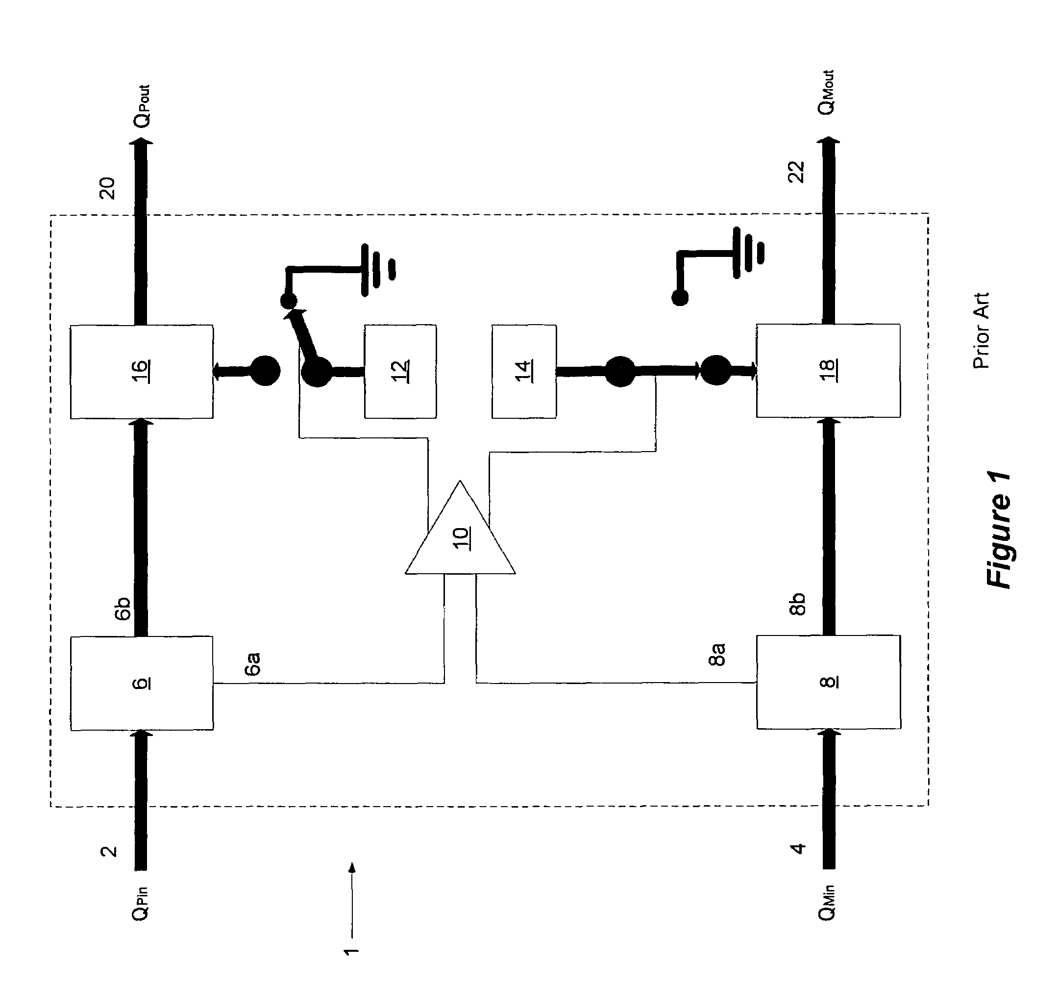
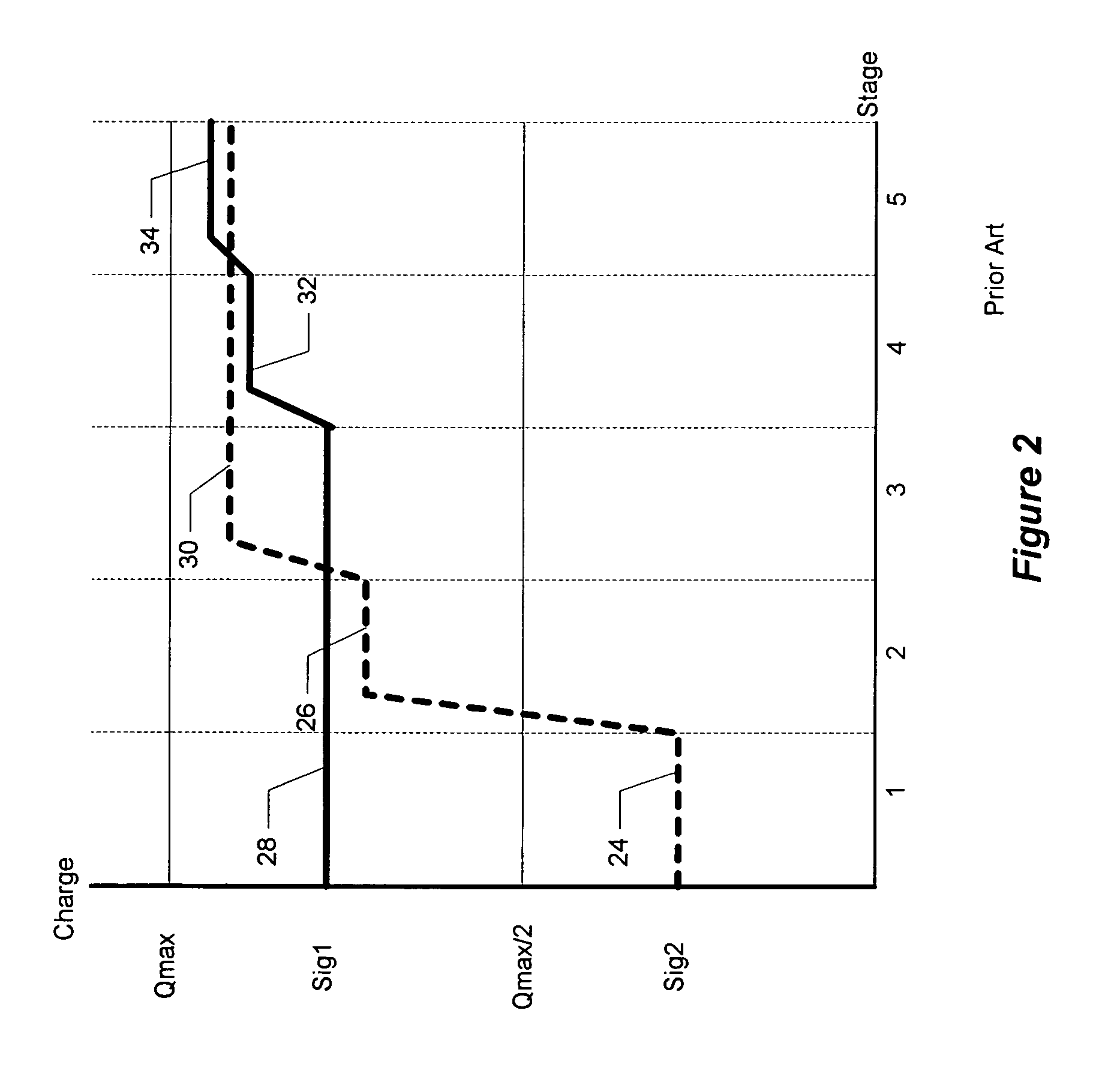
[0017]In order to make clear the advantages of the present invention, a brief description of the operation of a prior-art charge-domain pipelined ADC is first described. A typical pipeline stage in such an ADC is shown in FIG. 1. In this schematic representation, charge-transfer paths are shown as heavy lines with arrowheads, and normal (wired) connections are shown as single lines.

[0018]The details of the CCD structures are not important to this discussion and are not shown. Likewise the number of storage gates per pipeline stage can be varied from the number shown. The pipeline shown in this example has parallel CCD registers for the two components of the signal-charge pair. ADCs based on similar pipelines in which the signal-charge pair is interleaved in a single CCD register are also within the scope of the present invention.

[0019]Referring now to FIG. 1 a pipeline stage 1 operates as follows. A differential signal-charge pair QPin 2 and QMin 4 enter the stage as inputs either f...


PUM


Abstract

A pipelined analog-to-digital converter in which signal value samples are represented differentially by pairs of charges and which uses charge-coupled-devices (CCDs) for delay and arithmetic operations on the charges is presented. In the pipeline, each successive stage resolves an equal or smaller charge difference. After a certain number of pipeline stages, the common-mode component of the signal-charge pair is reduced. The pipeline stages following this common-mode-charge reduction stage have a reduced charge capacity and size, allowing more sensitive charge comparison. The result is improved A/D converter resolution and reduced power consumption.

Description

STATEMENTS REGARDING FEDERALLY SPONSORED RESEARCH[0001]This invention was made with government support under Contract No. F19628-00-C-0002 awarded by the Air Force. The government has certain rights in the invention.CROSS REFERENCE TO RELATED APPLICATIONS[0002]Not Applicable.FIELD OF THE INVENTION[0003]The present invention relates generally to analog-to-digital converters and more specifically to pipelined analog-to-digital converters employing charge-coupled devices (CCDs).BACKGROUND OF THE INVENTION[0004]Pipelined charge-domain analog-to-digital converters (ADCs) are known. In these ADCs, a sampled analog signal is represented as a sequence of charges or of charge-pair differences. The signal charges are stored, transported and processed in one or more CCD shift registers. In addition to charge storage and shifting, these charge-domain ADCs employ the operations of charge splitting, charge comparison and charge merging (addition) to perform analog-to-digital conversion.[0005]As i...

Claims


Application Information

Patent Timeline
IPC IPC(8): H03M1/06H03M1/12H03M1/14H03M1/44
CPCH03M1/0607H03M1/0682H03M1/146H03M1/44H03M1/12
Inventor ANTHONY, MICHAEL P.
Owner MASSACHUSETTS INST OF TECH
Why Eureka
Try Eureka