Method for making an ultra thin FDSOI device with improved short-channel performance

a technology of silicononinsulator and short-channel performance, which is applied in the direction of semiconductor devices, electrical equipment, transistors, etc., can solve the problems of difficult to achieve good short-channel control, difficult to reliably achieve with available processes, and off transistors, and achieve excellent ioff dc characteristics.

Inactive Publication Date: 2005-12-13
ADVANCED MICRO DEVICES INC +1
View PDF2 Cites 63 Cited by
  • Summary
  • Abstract
  • Description
  • Claims
  • Application Information

AI Technical Summary

Benefits of technology

[0006]It is therefore an object of this invention to provide a method for forming a Fully Depleted Silicon-On-Insulator device structure with a thin SO...

Problems solved by technology

For SOI devices having channel lengths below about 50 nm, in particular Fully Depleted Silicon On Insulator (FDSOI) devices, it is very difficult to achieve good short-channel control, i.e., to effectively shut off the transistors in the off state, without significantly thinning down the thickness of the buried layer an...

Method used


Image

  • Method for making an ultra thin FDSOI device with improved short-channel performance
  • Method for making an ultra thin FDSOI device with improved short-channel performance
  • Method for making an ultra thin FDSOI device with improved short-channel performance

Examples


Embodiment Construction

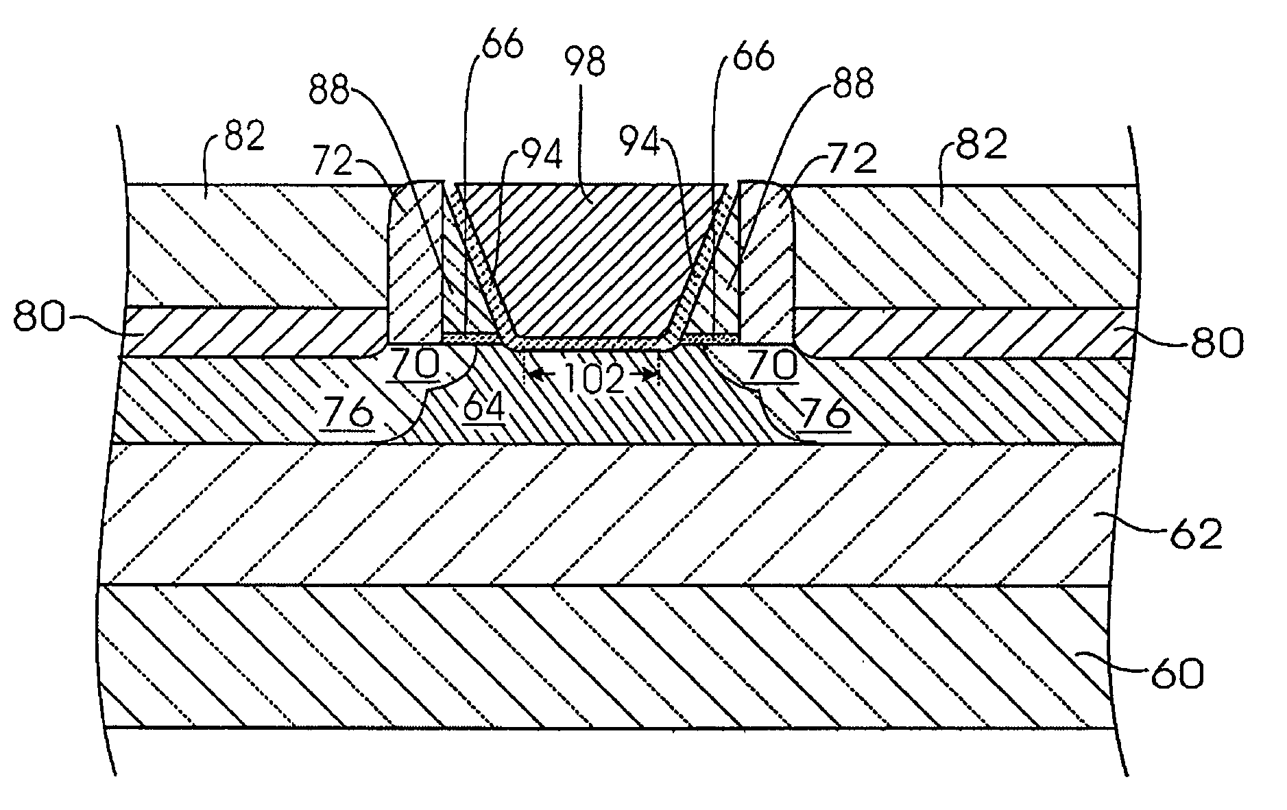
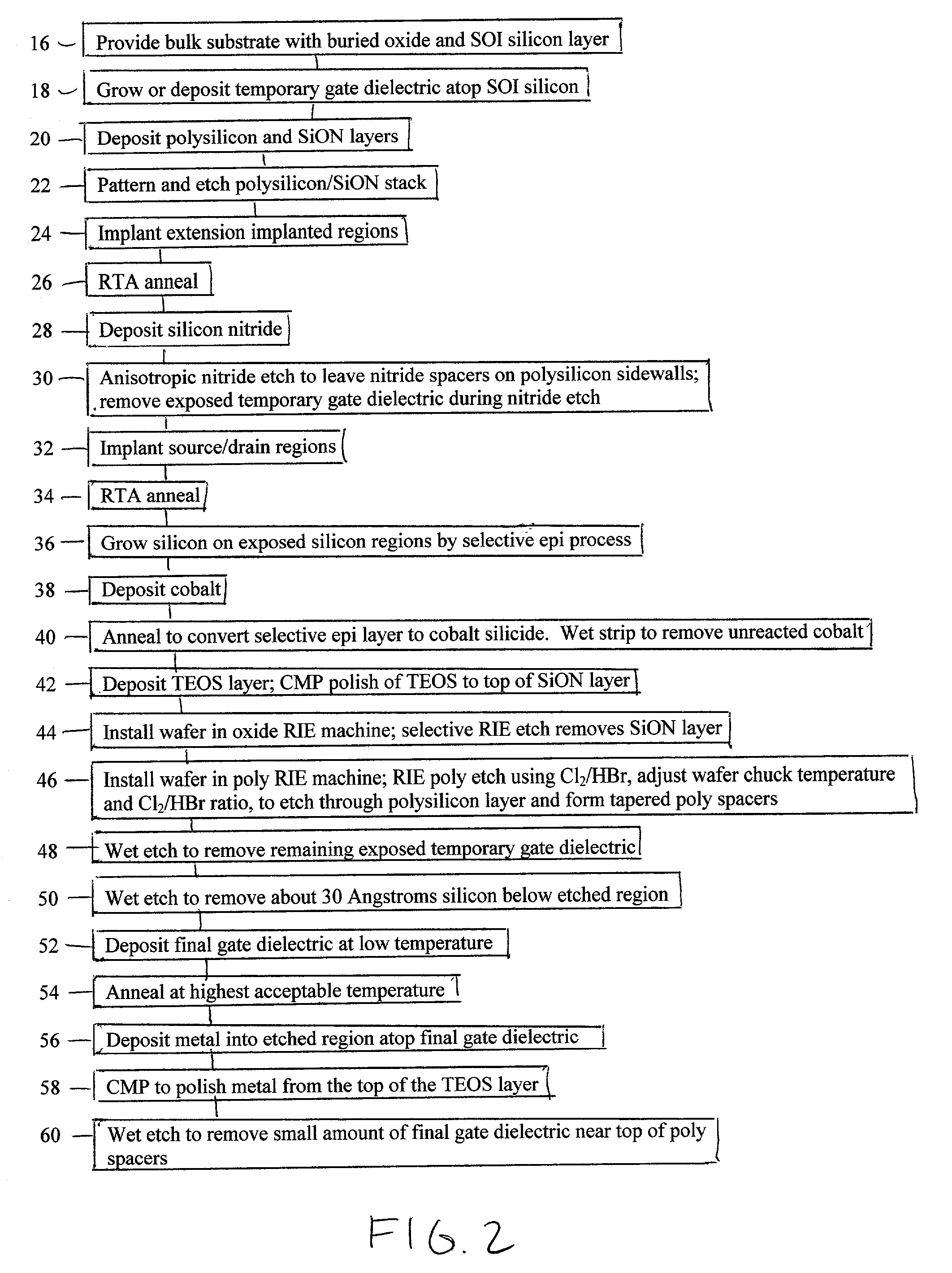
[0014]FIG. 2 shows a process flow for the inventive process. Intermediate structures resulting at stages of the process are illustrated in FIGS. 3a–3c.

[0015]Steps 16–42 provide the formation of a conventional MOS SOI structure using techniques known in the art.

[0016]In step 16, a bulk substrate 60 is provided having a buried oxide layer 62 thereon, usually undoped SiO2 with thickness of approximately 50–60 nm, and a thin undoped SOI silicon layer 64 of approximately 5–20 nm atop the buried oxide layer 62.

[0017]In step 18, temporary gate dielectric 66 is grown and / or deposited using standard methods atop the SOI silicon layer 64, comprising silicon dioxide alone or in combination with other dielectric such as silicon nitride, with a total equivalent oxide thickness of 0.6–2.0 mm.

[0018]In step 20, approximately 75–100 nm of polysilicon 65 is deposited atop the temporary gate dielectric 66, then 20–36 nm of SiON 67 is deposited atop the polysilicon.

[0019]In step 22, the polysilicon / Si...


PUM


Abstract

A method for forming a FDSOI device with channel length less than 50 nm with good short channel control. The gate has a tapered polysilicon spacer and a dielectric spacer. A polysilicon gate feature is formed and dielectric sidewall spacers are formed thereon. The polysilicon gate feature is then etched to form tapered poly features separated by a gap. A gate dielectric is deposited at low temperature, then metal is deposited into the gap to form the metal gate.

Description

CROSS-REFERENCE TO RELATED APPLICATION[0001]This application is related to U.S. Provisional Application No. 60 / 260,484, filed on Jan. 9, 2001.FIELD OF THE INVENTION[0002]This invention relates to semiconductor device manufacturing methods, and in particular to methods for forming ultra-thin Silicon-On-Insulator (SOI) device structures.BACKGROUND OF THE INVENTION[0003]As integrated circuit dimensions decrease and circuit speed increases, new transistor structures have been developed in order to yield good performance at the smaller dimensions. In particular, Silicon-On-Insulator (SOI) devices are known and are generally undoped or very lightly doped silicon on a low K dielectric. SOI devices are characterized by having the active device region insulated from the bulk substrate, generally by a buried oxide layer. The active device region is thereby said to be floating. SOI devices have been developed which consume less power than do bulk CMOS devices, and which operate at higher speed...

Claims


Application Information

Patent Timeline
IPC IPC(8): H01L21/336H01L29/00H01L29/423H01L29/786
CPCH01L29/42384H01L29/66545H01L29/66772H01L29/78621H01L29/78696
Inventor KRIVOKAPIC, ZORANCHERIAN, SUNNYHOLBROOK, ALLISON
Owner ADVANCED MICRO DEVICES INC
Why Eureka
Try Eureka