Semiconductor integrated circuit having pads layout for increasing signal integrity and reducing chip size

a technology of integrated circuits and pads, which is applied in the direction of semiconductor devices, semiconductor/solid-state device details, electrical devices, etc., can solve the problems of difficult to realize the reduction of chip size and the size of bonding pads that cannot be easily reduced, so as to increase signal integrity and reduce chip size

Active Publication Date: 2005-12-13
SAMSUNG ELECTRONICS CO LTD
View PDF9 Cites 3 Cited by
  • Summary
  • Abstract
  • Description
  • Claims
  • Application Information

AI Technical Summary

Benefits of technology

[0008]Exemplary embodiments of the present invention provide a semiconductor integrated circuit device having a bonding pads layout structure capable of increasing signal integrity and reducing a chip size.
[0016]The pad layout structure of the semiconductor integrated circuit device may increase a signal integrity for signals input and output through circuits of a peripheral circuit region, by using a pads layout on only one side of the chip, and may reduce a chip size by using a concentrated layout of bonding pads and circuit elements constituting the peripheral circuit region on only one side of the chip.

Problems solved by technology

That is, even if the size of a chip may be reduced, a size of the bonding pads may not be easily reduced because of problems such as reinvestment in bonding equipment and test equipment using the bonding pads.
In wire bonding pads of an edge pad layout system, there may be no wire formed over an upper part of a memory cell array region 11, but a reduction of the chip size may be difficult to realize because the pads are disposed on several sides of the chip 100.

Method used


Image

  • Semiconductor integrated circuit having pads layout for increasing signal integrity and reducing chip size
  • Semiconductor integrated circuit having pads layout for increasing signal integrity and reducing chip size
  • Semiconductor integrated circuit having pads layout for increasing signal integrity and reducing chip size

Examples


Embodiment Construction

[0024]The present invention and exemplary embodiments thereof are more fully described below with reference to the accompanying drawings. This invention may, however, be embodied in many different forms and should not be construed as being limited to the exemplary embodiments set forth herein; rather, these exemplary embodiments are provided so that this disclosure is thorough and complete, and conveys the concept of the invention to those skilled in the art.

[0025]According to exemplary embodiments of the present invention, a semiconductor integrated circuit device having one-side layout structure of bonding pads is provided.

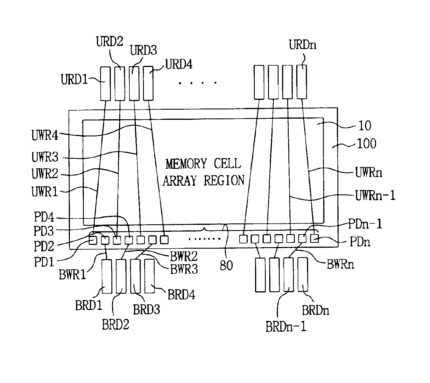
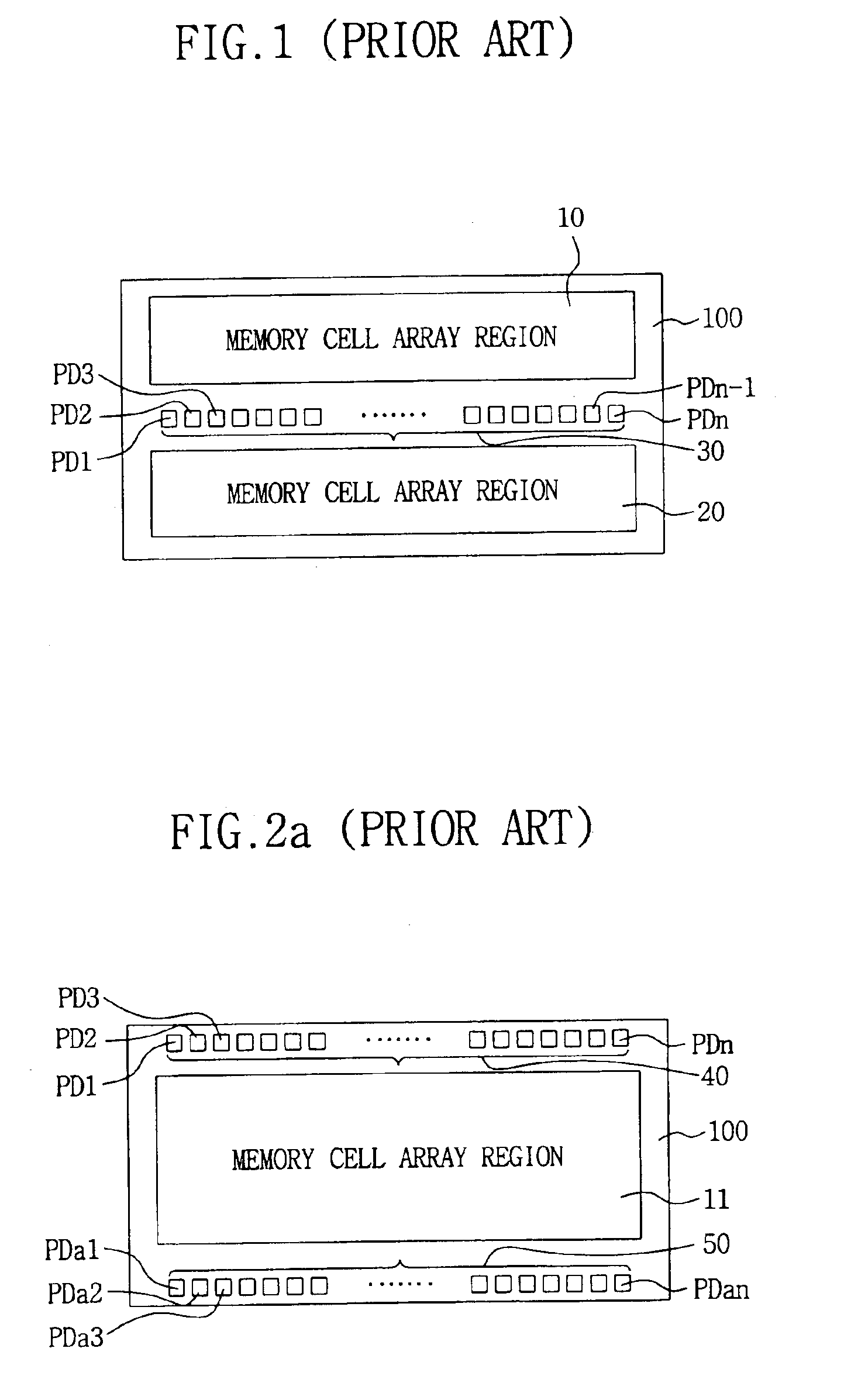
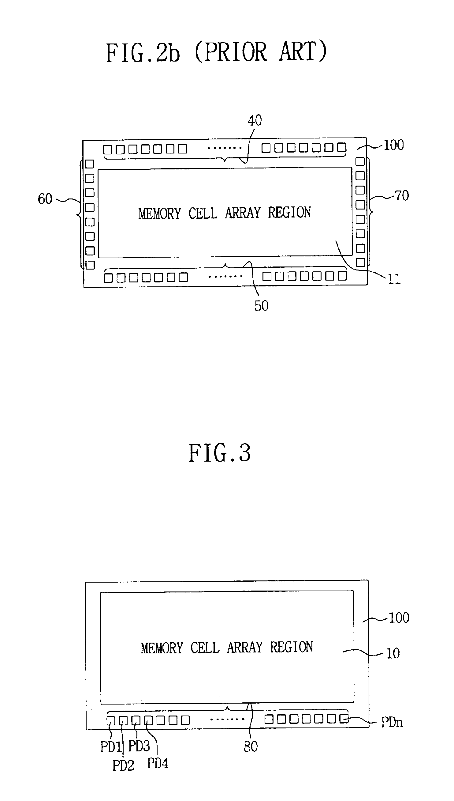
[0026]FIG. 3 is a plan view illustrating the exterior of a semiconductor integrated circuit device having a one side pad layout structure according to an exemplary embodiment of the present invention. Referring to FIG. 3, the semiconductor integrated circuit device includes a semiconductor chip 100, and the semiconductor chip 100 has a memory cell array region 1...


PUM


Abstract

A semiconductor integrated circuit device includes a semiconductor chip having a memory cell array region surrounded with a peripheral circuit region and includes a plurality of bonding pads disposed at least in one row on only one side of the semiconductor chip. The circuit device may include first leads group disposed adjacent to the bonding pad side and a second leads group disposed opposite the first leads group. The second leads group may be formed over a portion of the semiconductor chip (lead-on-chip structure). A plurality of bonding wires connect the first and second leads group with the plurality of bonding pads respectively.

Description

[0001]This U.S. nonprovisional patent application claims priority under 35 U.S.C. §119 of Korean Patent Application 2003-11686 filed on Feb. 25, 2003, the entire contents of which is hereby incorporated by reference.FIELD OF THE INVENTION[0002]The present invention relates to a semiconductor integrated circuit device, and more particularly to a pad layout and a wire bonding in a semiconductor integrated circuit device, such as a semiconductor memory device etc.DESCRIPTION OF THE RELATED ART[0003]A semiconductor integrated circuit, such as a semiconductor memory device generally has bonding pads on an upper surface of a chip to allow for an external electrical connection with another chip. Electrical signals, such as command input signals, data read and data write operation signals are input or output the chip through the bonding pads.[0004]Even though a degree of integration for elements mounted in the semiconductor chip may be increased, e.g., doubled, the number of bonding pads ma...

Claims


Application Information

Patent Timeline
Patent Type & Authority Patents(United States)
IPC IPC(8): H01L23/50H01L21/60
CPCH01L23/50H01L24/06H01L24/49H01L2224/05599H01L2224/48H01L2224/4912H01L2224/49171H01L2224/85399H01L2924/01006H01L2924/01082H01L2924/14H01L24/48H01L2924/00014H01L2924/01033H01L2224/45099H01L2224/05554H01L2224/4811H01L2924/10161H01L21/60
Inventor LEE, HO-CHEOL
Owner SAMSUNG ELECTRONICS CO LTD
Why Eureka
Try Eureka