Reduced size dielectric loaded spiral antenna

a spiral antenna and dielectric loading technology, applied in the direction of resonant antennas, radiating elements structural forms, protective materials radiating elements, etc., can solve the problems of limited design of spiral antennas, use of dielectric loading in previous designs with limited success, etc., to reduce the required antenna diameter, reduce the length of printed circuit baluns, and reduce the antenna input impedance

Inactive Publication Date: 2005-12-13
THE UNITED STATES OF AMERICA AS REPRESENTED BY THE SECRETARY OF THE NAVY
View PDF5 Cites 14 Cited by
  • Summary
  • Abstract
  • Description
  • Claims
  • Application Information

AI Technical Summary

Benefits of technology

[0008]The present invention overcomes some of the disadvantages of the past including those mentioned above in that it comprises a very efficient and effective spiral antenna having a substantial reduction in size while providing for the desired frequency of operation.
[0010]Two unique features of the spiral antenna design provide for size reduction at a given lowest required frequency of operation. The spiral antenna has dielectric material layers positioned on both side of the antenna's metal arms. This enables a reduction in the required size of the antenna diameter.
[0011]In addition, the antenna input impedance is reduced from the normal 100 ohm input impedance to approximately 50 ohms due the dielectric material. This reduces the length of the printed circuit balun needed to provide signal balance to the spiral antenna. The design of the spiral antenna, virtually eliminates balun circuit length normally required to provide impedance taper which is typically from 100 ohms to 50 ohms. The balun has minimal length, with the overall antenna length being determined by the thickness by a microwave energy absorber utilized by the spiral antenna.

Problems solved by technology

In the past the design of spiral antennas has been limited by two criteria with respect to the spiral antenna's lowest desired frequency of operation.
Previous designs for spiral antenna size reduction have used dielectric loading with limited success.

Method used


Image

  • Reduced size dielectric loaded spiral antenna
  • Reduced size dielectric loaded spiral antenna
  • Reduced size dielectric loaded spiral antenna

Examples


Embodiment Construction

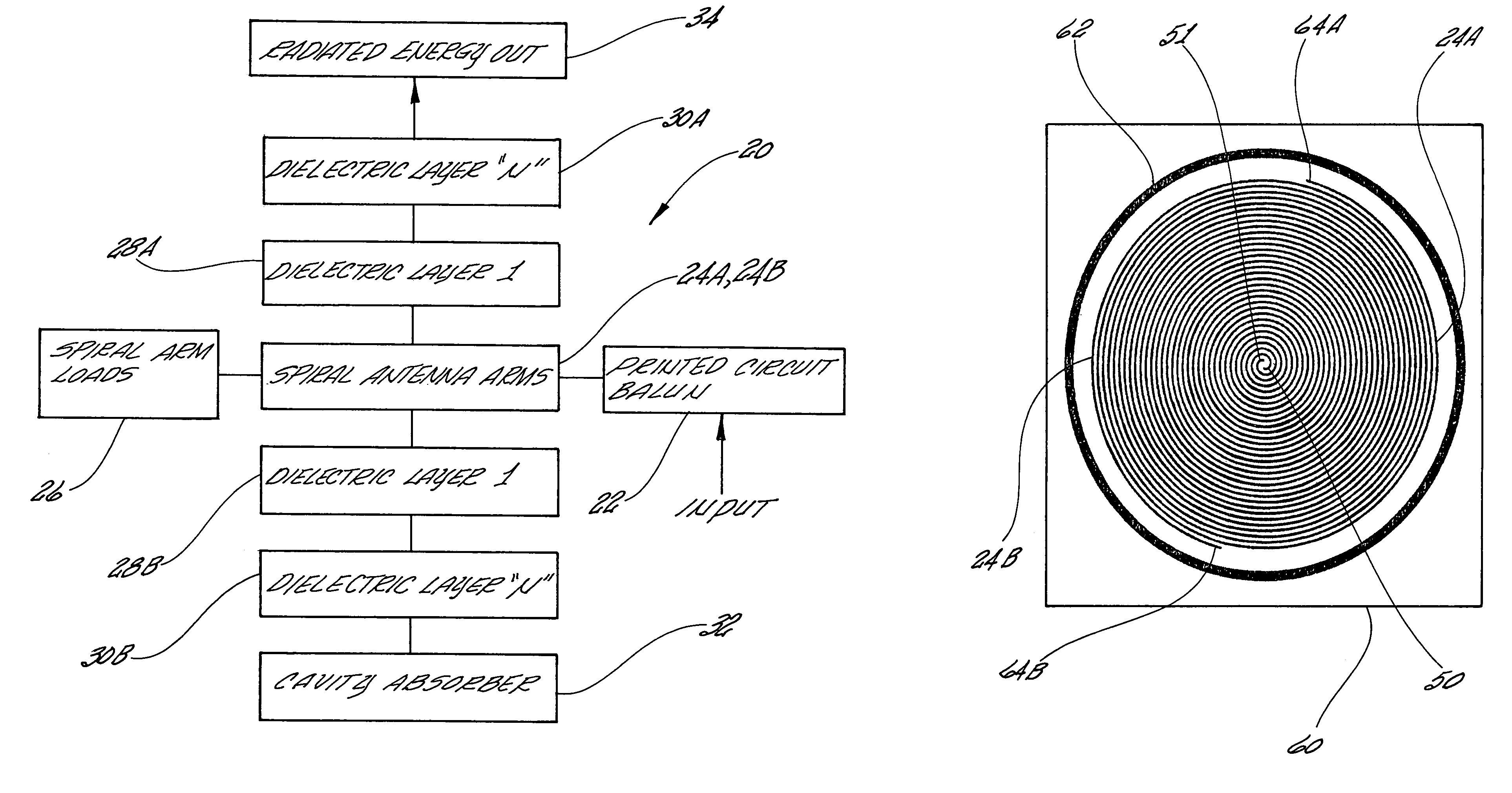
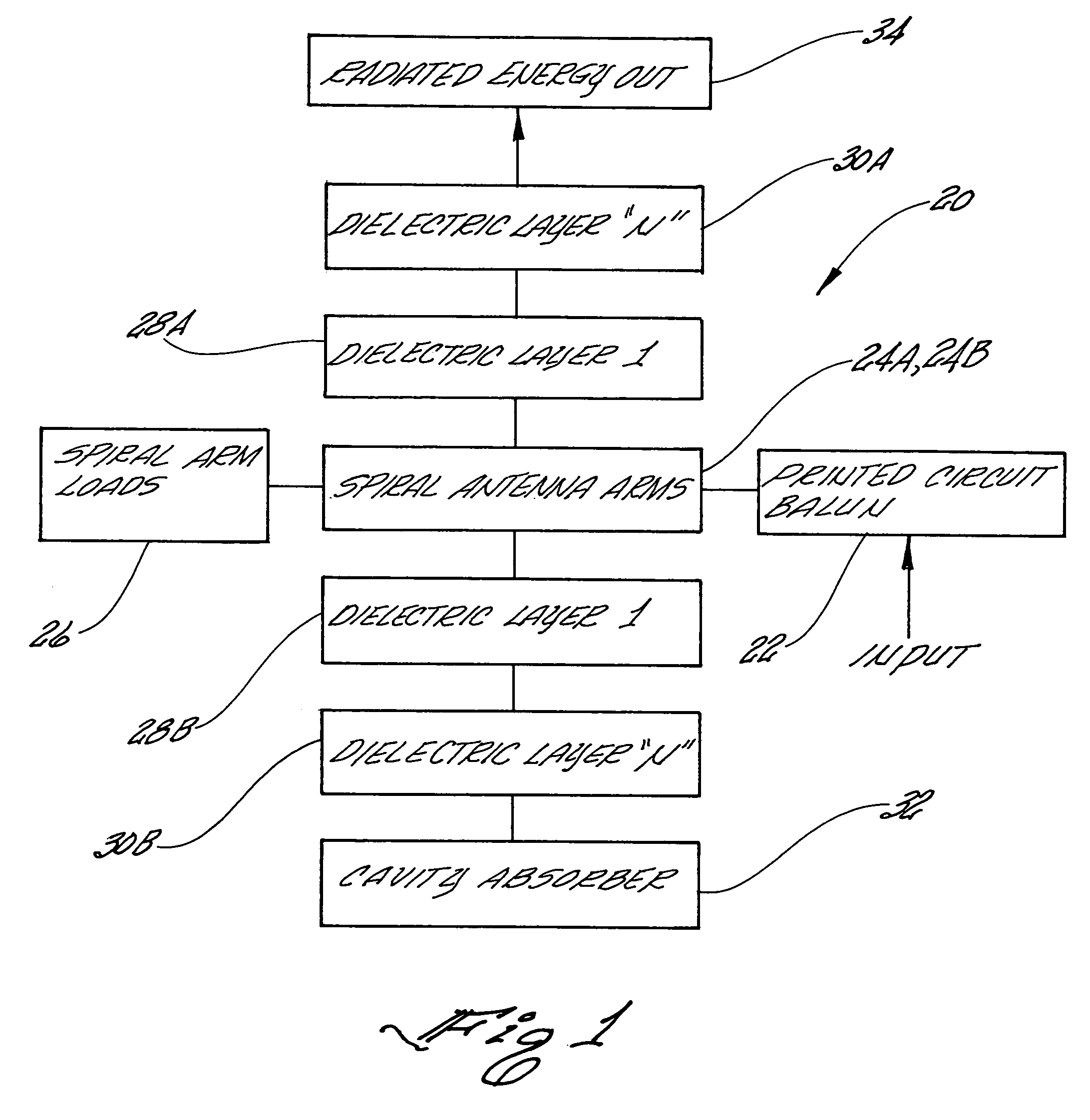
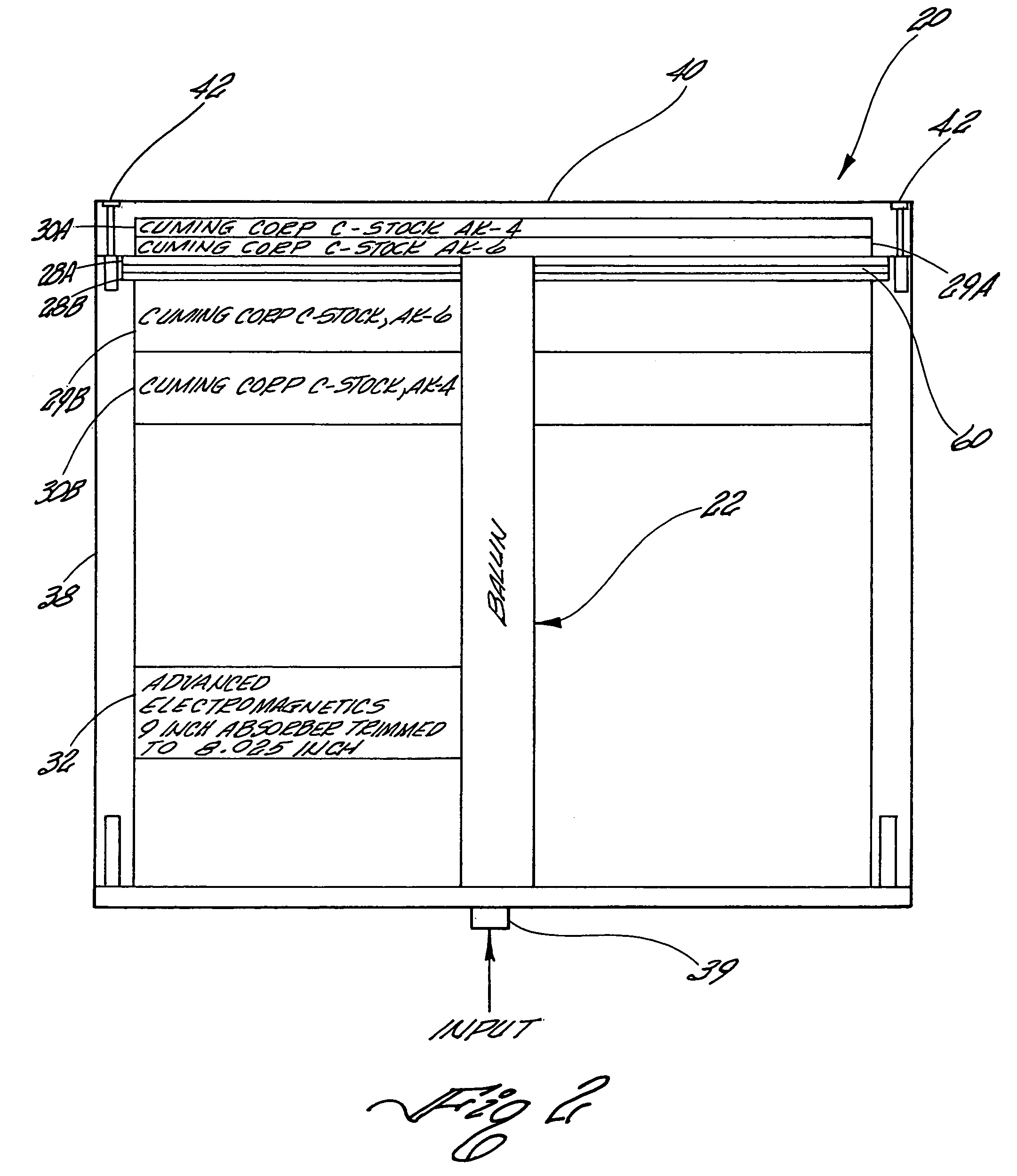
[0014]Referring to FIGS. 1, 3A, 3B and 3C, FIG. 1 is a block diagram illustrating the spiral antenna 20 comprising the present invention. The antenna can have either an archimedean spiral geometry as shown in FIG. 3C or a logarithmic spiral geometry. The spiral antenna 20 has a pair of spiral arms 24A and 24B mounted on a dielectric substrate 60 (FIG. 3C). The antenna arms 24A and 24B are respectively connected to a balun 22 (depicted in FIGS. 3A and 3B) by antenna signal arm inputs 50 and 51 which are positioned at the center of spiral antenna 20. Each of the antenna arms 24A and 24B of spiral antenna 20 is also connected to a spiral arm load 26 at a pair of load connection terminals 64A and 64B. As shown in FIG. 3C, the antenna arm signal inputs 50 and 51 are located at the inner end of antenna arms 24A and 24B, while the load connection terminals 64B and 64B are located at the outer end of antenna arms 24A and 24B.

[0015]The spiral arm loads 26 used in the preferred embodiment are...


PUM


Abstract

A spiral antenna having a pair of antenna arms mounted on a dielectric substrate. A balun is included to connect the antenna which has an impedance of 100 ohms to a 50 ohm cable. Unique features of the spiral antenna design provide for size reduction at a given lowest required frequency of operation. The spiral antenna has dielectric material layers positioned on both side of the antenna's metal arms. In addition, the antenna input impedance is reduced from the normal 100 ohm input impedance to approximately 50 ohms due the dielectric material.

Description

BACKGROUND OF THE INVENTION[0001]1. Field of the Invention[0002]The present invention relates generally to a spiral antenna. More specifically, the present invention relates to an archimedean spiral antenna which has a reduction in the required size of its antenna diameter and length.[0003]2. Description of the Prior Art[0004]In the past the design of spiral antennas has been limited by two criteria with respect to the spiral antenna's lowest desired frequency of operation. First, the diameter for a sum type mode of operation (simple cosine power pattern) has to be a minimum of one wavelength divided by PI. The length of a typical spiral antenna assembly with an embedded printed circuit balun feed need to be one half wavelength.[0005]For example, a spiral antenna which is required to operate at one Gega-hertz (GHz) without a serious decrease in gain would result in a spiral antenna with a diameter of 3.75 inches and a length of 6.0 inches.[0006]However, for this example, there is a ...

Claims


Application Information

Patent Timeline
Patent Type & Authority Patents(United States)
IPC IPC(8): H01Q1/26H01Q1/36H01Q1/38H01Q1/40H01Q9/27
CPCH01Q1/38H01Q1/40H01Q9/27
Inventor NEEL, MICHAEL M.
Owner THE UNITED STATES OF AMERICA AS REPRESENTED BY THE SECRETARY OF THE NAVY
Why Eureka
Try Eureka