

Switching power supply device and switching power supply system
- Summary
- Abstract
- Description
- Claims
- Application Information
AI Technical Summary
Benefits of technology
Problems solved by technology
Method used
Image

Examples
second embodiment
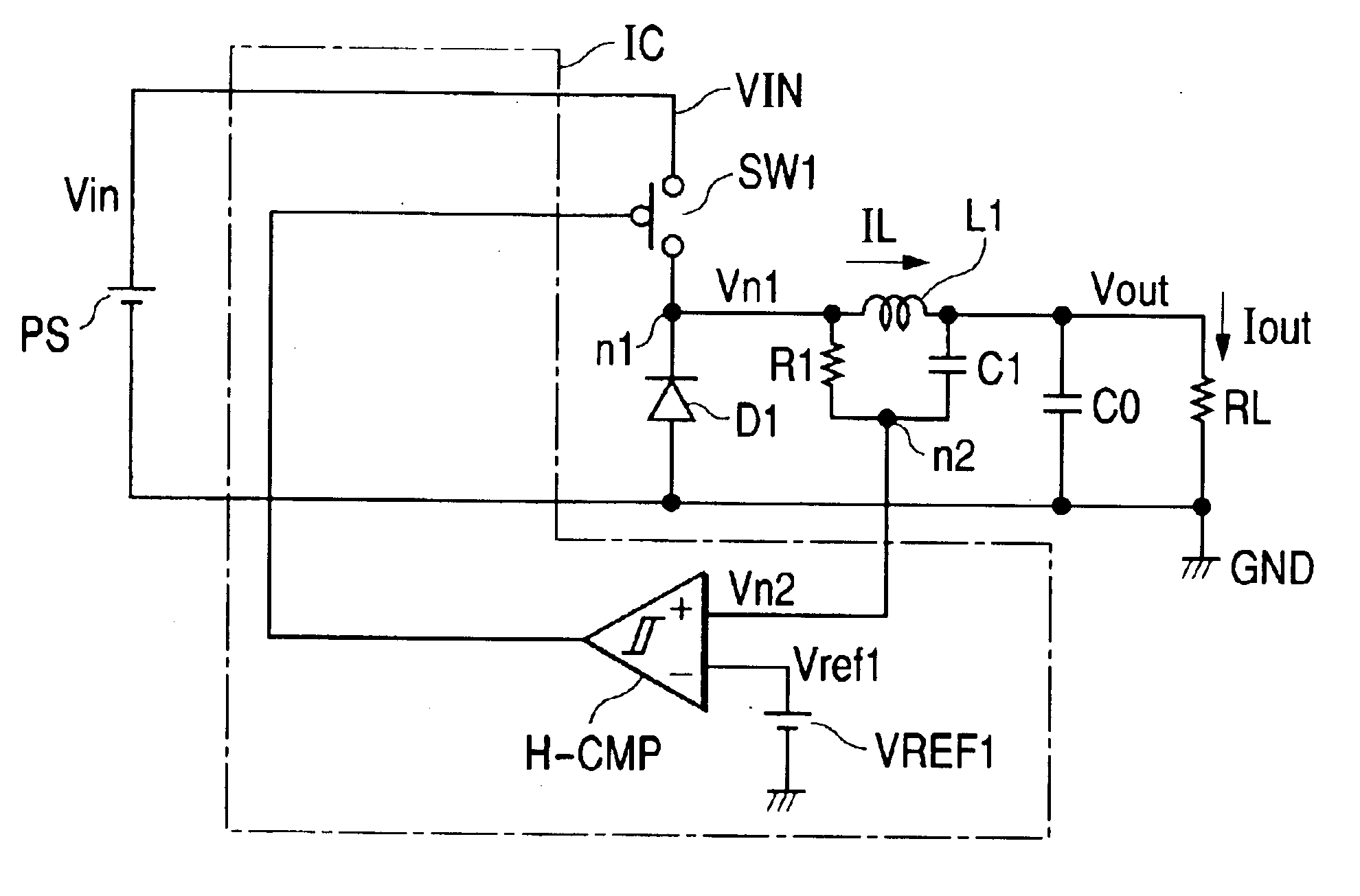
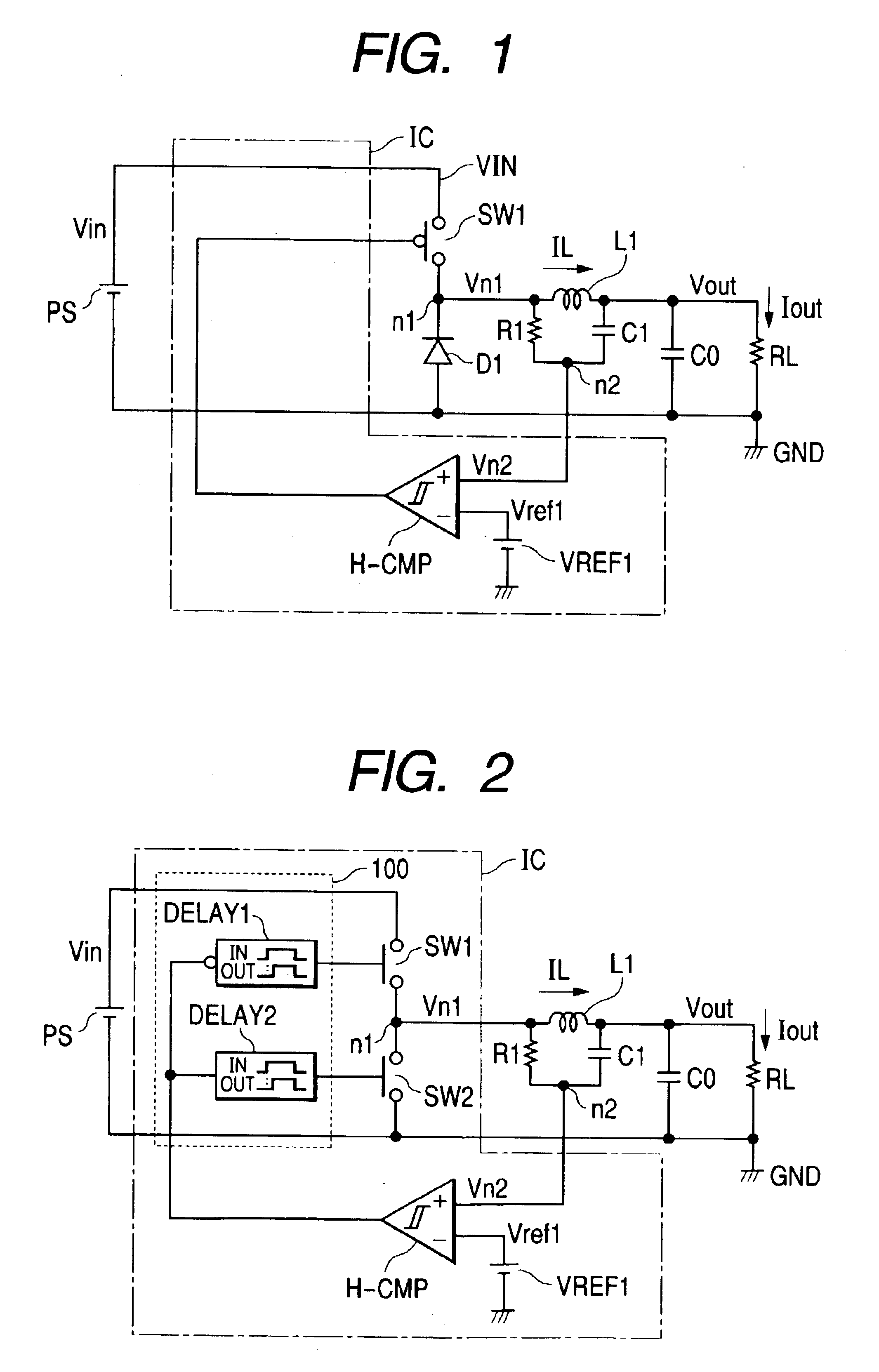
[0064]However, this part is never limited only to the structure described above and it may use, in place of the diode D1, the switch SW2 which complementarily turns ON and OFF against the switch SW1, as in the case of the switching regulator of the present invention illustrated in FIG. 2.
[0065]But, in this case, it is required to provide the dead band using the delay circuits DELAY1, DELAY2 or the like in the switching control circuit 100 in order to prevent that the switches SW1 and SW2 simultaneously turn ON and a heavier current flows through the voltage input terminal VIN and the ground point GND.
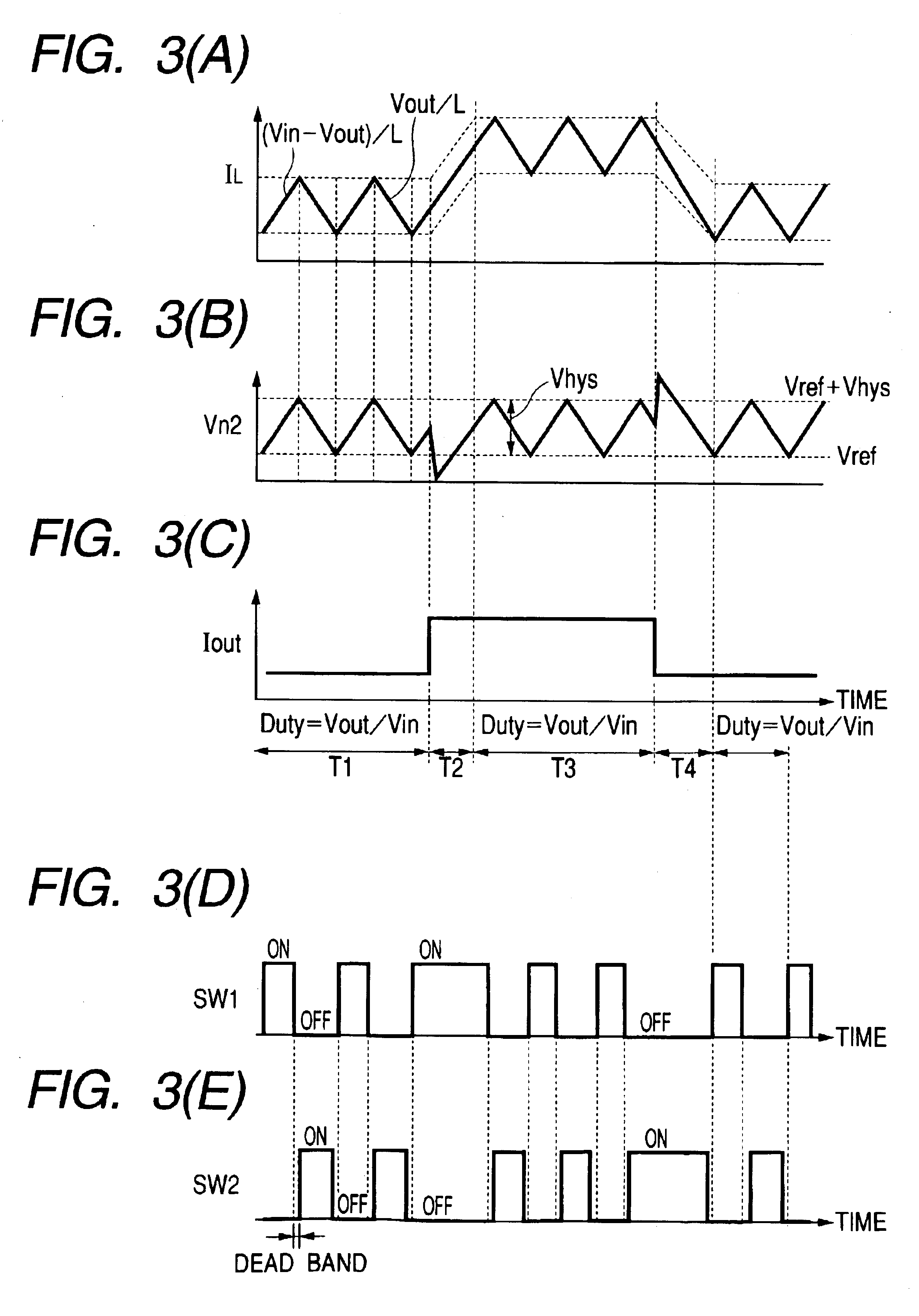
[0066]In the case where a through-current does not flow because the switches SW1 and SW2 are operated complementarily, the switching control circuit is configured, although not particularly restricted, as designated as 100 in FIG. 2. The delay circuit thereof has the input / output relationship as illustrated in FIG. 15A. Accordingly, an output is delayed for the incoming L→H input but th...
third embodiment
[0079]FIG. 4A illustrates the switching regulator of the present invention.
[0080]This embodiment uses an ordinary comparator CMP through replacement of the comparator H-CMP having the hysteresis characteristic used in the second embodiment, and switches the reference voltage VHYS to be inputted to this comparator. In more practical, the switching regular of this embodiment is provided with a reference voltage source VREF1 and a reference voltage generating circuit 120 consisting of the serial resistors R6, R7, R8 for dividing the reference voltage Vref1 generated by the reference voltage source VREF1 and a resistance dividing circuit 121 consisting of the switch SW3 provided in parallel with the resistor R8. In this structure, the potential of the connection node n3 of the resistor R6 and resistor R7 is impressed to the inverted input terminal of the comparator CMP as the reference voltage VHYS and the comparator CMP seems to have virtual hysteresis characteristic by changing the re...
fourth embodiment
[0083]FIG. 4C illustrates the switching regulator of the present invention.
[0084]This embodiment realizes the switching regulator of the type having the hysteresis characteristic by using two ordinary comparators. In more practical, the hysteresis characteristic can be attained by inputting the potential of node n2 to the non-inverted input terminals of the comparators CMP1, 2, inputting the reference voltage Vref1 generated by the reference power source VREF1 to the non-inverted input terminal of the comparator CMP1, inputting the voltage Vref1−Vhys divided from the reference voltage Vref1 with the series resistors R8, R9 to the non-inverted input terminal of the comparator CMP2, inputting the voltage obtained by inverting an output of the comparator CMP1 to the reset terminal of the RS flip-flop circuit 103 and inputting an output of the comparator CMP2 to the set terminal of the RS flip-flop circuit 103. In this embodiment, hen the potential of the node n2 becomes higher than the...
PUM
 Abstract
Description
Claims
Application Information