Method and apparatus for building up large scale on chip de-coupling capacitor on standard CMOS/SOI technology

a technology of decoupling capacitor and chip, which is applied in the direction of electrical apparatus, semiconductor devices, semiconductor/solid-state device details, etc., can solve the problems of sudden current drain, limiting the clock speed at which the device can be satisfactorily operated, and rapid changes in power supply voltage and spikes in lead circuits and die circuits, etc., to achieve easy implementation, increase chip area, and low cost

Inactive Publication Date: 2006-01-03
HEWLETT PACKARD DEV CO LP
View PDF5 Cites 5 Cited by
  • Summary
  • Abstract
  • Description
  • Claims
  • Application Information

AI Technical Summary

Benefits of technology

[0019]In comparison to known prior art, certain embodiments of the invention are capable of achieving certain aspects, including some or all of the following: (1) the technique is easily implemented (2) at a very low cost; and (3) no need to increase the chip area to accommodate a large capacitance. Those skilled in the art will appreciate these and other advantages and benefits of various embodiments of the invention upon reading the following detailed description of a preferred embodiment with reference to the below-listed drawings.

Problems solved by technology

The switching operations between no current and peak current is very rapid and may cause rapid changes in the power supply voltage and spikes within the lead circuits and die circuits.
Such induced voltage and current variations cause malfunctions of the integrated circuit and may severely limit the clock speed at which the device can be satisfactorily operated.
The problem is particularly relevant in devices having a large number of leads, where many leads may be simultaneously switched ON to cause a large, sudden current drain.
If the de-coupling capacitance is not enough, the inductance of the power delivery line might cause voltage dipping which could result in the malfunction of the chip.
Decoupling capacitors are frequently used in the supply rail of the on-chip cache memory blocks inside the processor chip due to high current demand during cache access from the CPU.
In today's VLSI processor class, such as the Pentium 4 or PowerPC, the on-chip cache often occupies a large amount of chip area.
Integrated circuits operating at such high frequencies are frequently susceptible to various forms of interference, such as, signal coupling and radio frequency interference.
However, the solutions put forth by the prior art tend to be costly.

Method used


Image

  • Method and apparatus for building up large scale on chip de-coupling capacitor on standard CMOS/SOI technology
  • Method and apparatus for building up large scale on chip de-coupling capacitor on standard CMOS/SOI technology
  • Method and apparatus for building up large scale on chip de-coupling capacitor on standard CMOS/SOI technology

Examples


Embodiment Construction

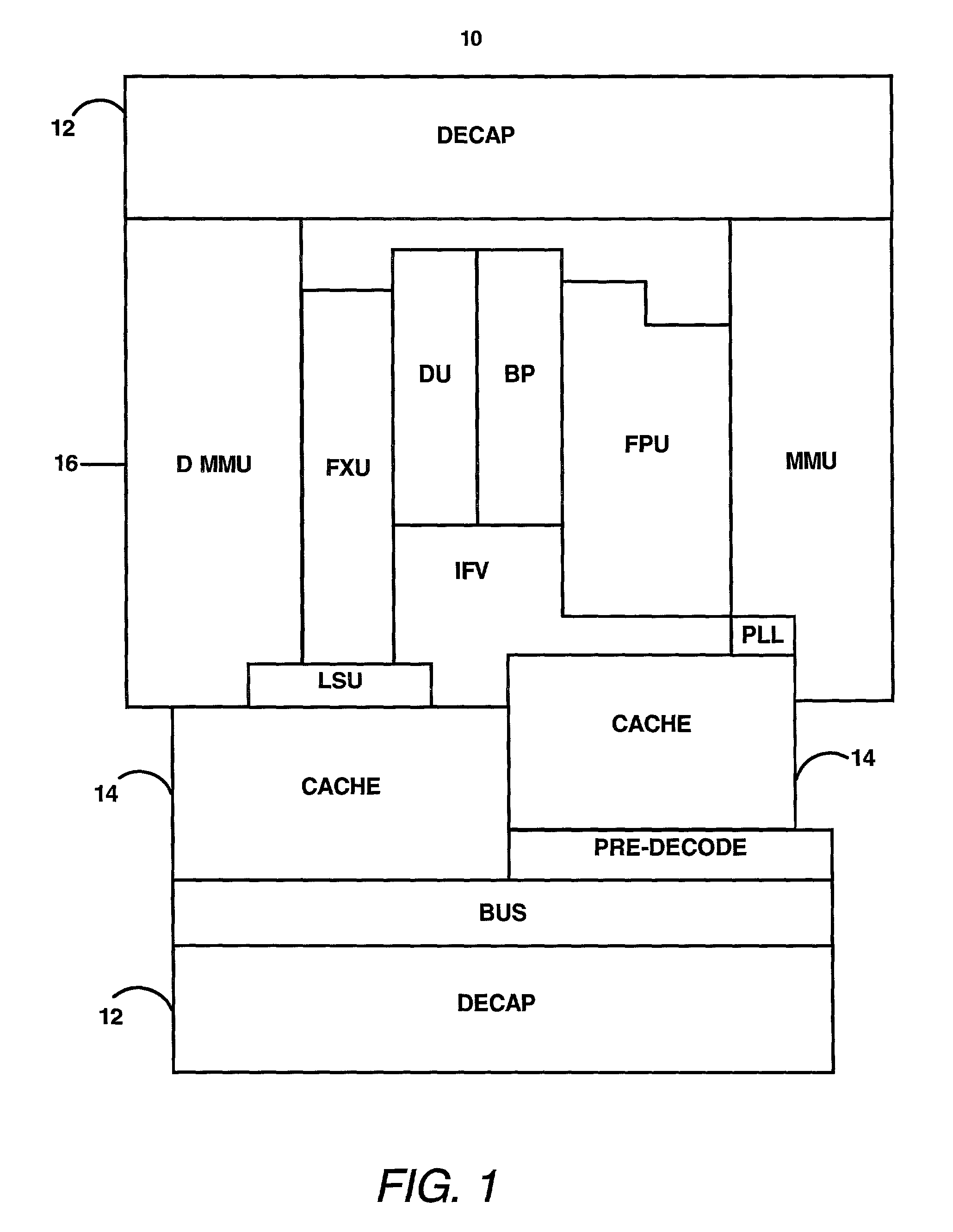
[0025]In the following detailed description, numerous specific details are set forth in order to provide a thorough understanding of the present invention. However, it will be apparent to one of ordinary skill in the art that these specific details need not be used to practice the present invention. In other instances, well known structures, interfaces, and processes have not been shown in detail in order not to unnecessarily obscure the present invention.

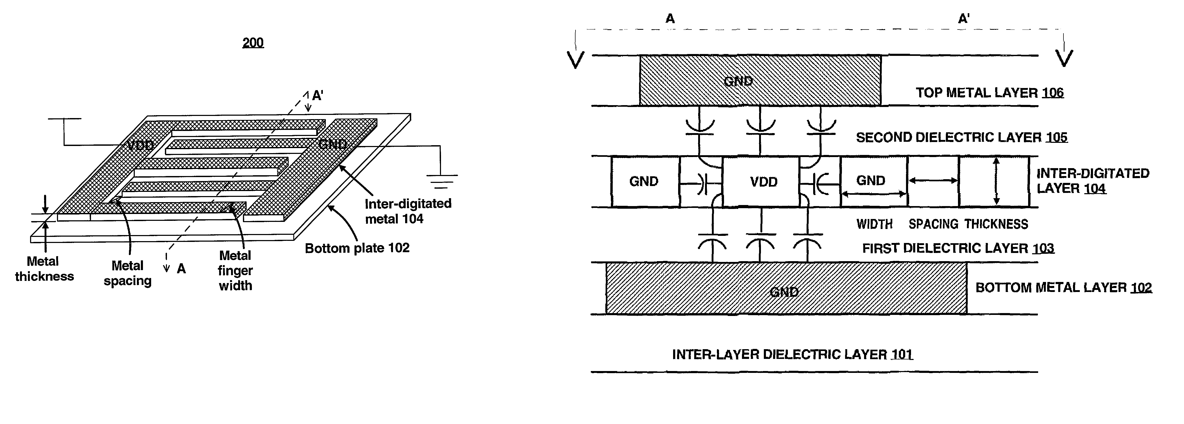
[0026]Decoupling capacitors and methods for fabricating such capacitors are disclosed. In the following description, numerous specific details are set forth, such as materials, thickness, processing sequences, etc., in order to provide a thorough understanding of the present invention. However, one skilled in the art would understand that the present invention may be practiced without these specific details. In other instances, well known processing steps and device structures have not been described in detail in order to avoid unn...


PUM


Abstract

The apparatus and method for forming de-coupling capacitors on top of SOC VLSI chip. The introduced large amount of de-coupling capacitor is intended to solve the power delivery problem of highly integrated and powered VLSI chip, especially in the Silicon-On-Insulator (SOI) technology. This invention proposes a design scheme which could utilize virtually unused area to build efficient de-coupling capacitors without introducing additional manufacture cost. This design scheme is especially effective when the VLSI technology is scaled down further.

Description

FIELD OF THE INVENTION[0001]This invention relates generally to a semiconductor device and in particular to improving decoupling capacitor integrated circuits built onto a memory device.BACKGROUND OF THE INVENTION[0002]Modern semiconductor devices including integrated circuit devices have electrically conductive leads and output drivers which are switched ON and OFF. The switching operations between no current and peak current is very rapid and may cause rapid changes in the power supply voltage and spikes within the lead circuits and die circuits. Such induced voltage and current variations cause malfunctions of the integrated circuit and may severely limit the clock speed at which the device can be satisfactorily operated. The problem is particularly relevant in devices having a large number of leads, where many leads may be simultaneously switched ON to cause a large, sudden current drain.[0003]The goal of decoupling capacitors is to provide a condition whereby the actual ranges ...

Claims


Application Information

Patent Timeline
Patent Type & Authority Patents(United States)
IPC IPC(8): H01L21/8242H01L21/20H01L23/522H01L27/08
CPCH01L27/0805H01L23/5223H01L2924/0002H01L2924/00
Inventor KU, JOSEPH W.VOORDE, PAUL VANDE
Owner HEWLETT PACKARD DEV CO LP
Why Eureka
Try Eureka