Filter circuit

a filter circuit and filter circuit technology, applied in the field of filter circuits, can solve the problems of large circuit size, large power consumption, complicated circuit for inspecting the peak of analog signals, etc., and achieve the effects of reducing circuit size and power consumption, improving the accuracy of receiving a receive signal, and processing a signal with eas

Inactive Publication Date: 2006-01-03
SHARP KK
View PDF13 Cites 46 Cited by
  • Summary
  • Abstract
  • Description
  • Claims
  • Application Information

AI Technical Summary

Benefits of technology

[0017]The present invention is devised to solve the above problem. The objective is to provide a filter circuit which is capable of reducing circuit size and power consumption, improving the accuracy of receiving a receive signal even in the case of small circuit size and power consumption, and processing a signal with ease in the following circuit.

Problems solved by technology

However, in this case, the circuit becomes larger.
Further, the shorter the chip interval length Tc, the higher operating speed is required, resulting in larger power consumption.
Although the construction disclosed in the above publication reduces power consumption of a baseband processing section by suppressing an operating speed of the A / D convertor, a circuit for inspecting a peak of an analog signal becomes complicated.
Since a peak value of an analog output signal is detected and is subjected to A / D conversion, accuracy for detecting a peak value is low in spite of the complicated circuit.
Consequently, an analog spread spectrum receive signal cannot be accurately modulated.
Therefore, the power consumption of the adder becomes larger.
Consequently, the construction becomes complicated and the power consumption is increased.
Moreover, regarding the construction disclosed in Japanese Published Examined Patent No. 2773075, any problem occurs in the case of the PN code having a small number of taps.
However, for practical use as a matched filter, it is necessary to add a partial correlation value for 256 to 512 times and to cumulate a larger amount of charge, resulting in degradation in S / N.

Method used


Image

  • Filter circuit
  • Filter circuit
  • Filter circuit

Examples


embodiment 1

[0042]Referring to FIG. 1, the following explanation describes Embodiment 1 of the present invention.

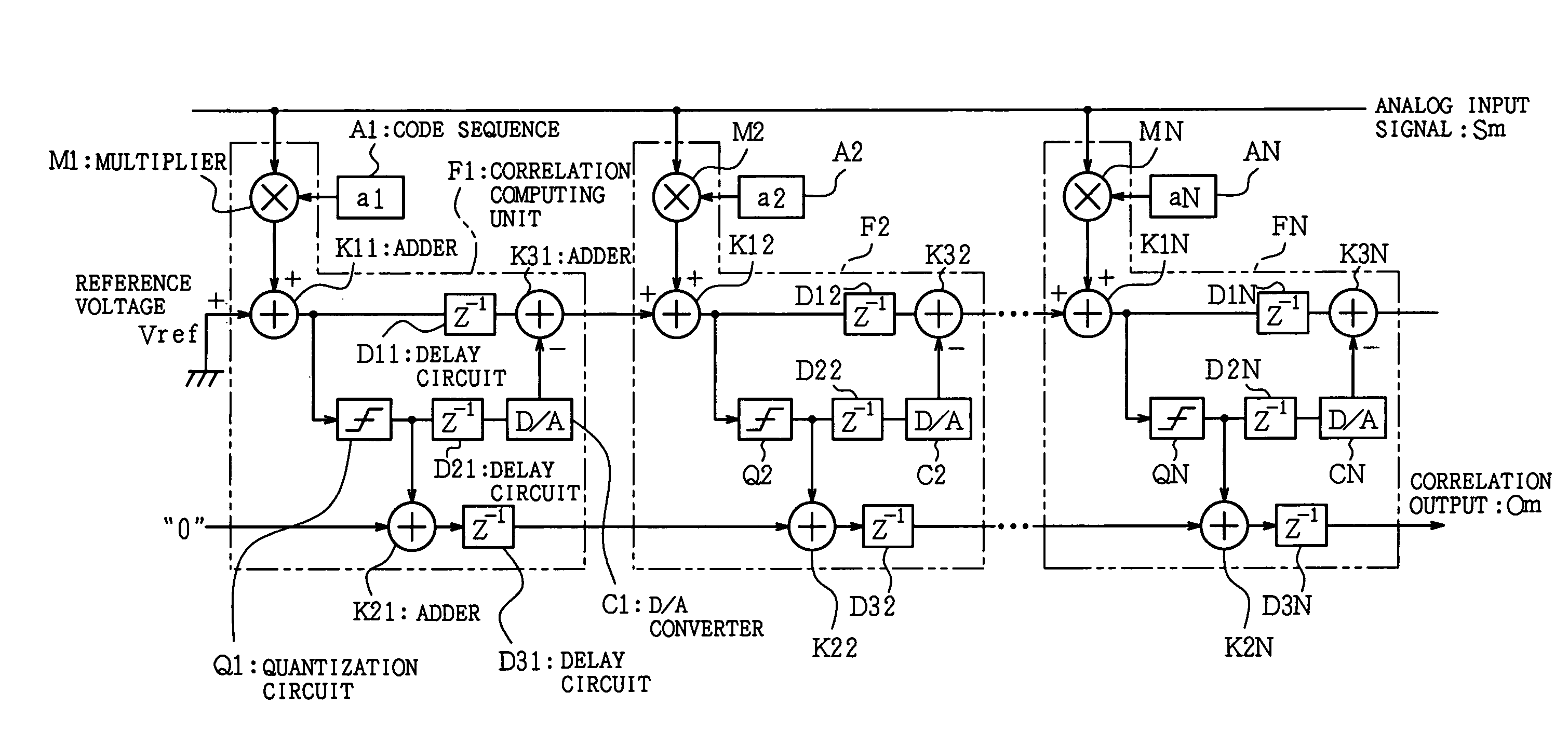
[0043]FIG. 1 is a block diagram showing an electric construction of an FIR filter in accordance with Embodiment 1 of the present invention. Unlike a filter shown in FIG. 18, the FIR filter has a filter shown in FIG. 19 serving as a fundamental construction, and is constituted by N-stage correlation computing unit Fj (j=1, 2, . . . , N, and hereinafter, subscript j is omitted when collectively called) connected in series. An analog input signal Sm, which is subjected to sampling with a chip period Tc at a timing m, is commonly inputted to all the correlation computing units F.

[0044]Each correlation computing unit Fj is constituted by a multiplier Mj and a code sequence Aj serving as computing means; an adder K1j serving as a first adding means; a quantization circuit Qj serving as a quantizing means; a delay circuit D1j serving as a first delay means; a delay circuit D2j serving as a ...

embodiment 2

[0055]Referring to FIG. 2, the following explanation describes Embodiment 2 of the present invention.

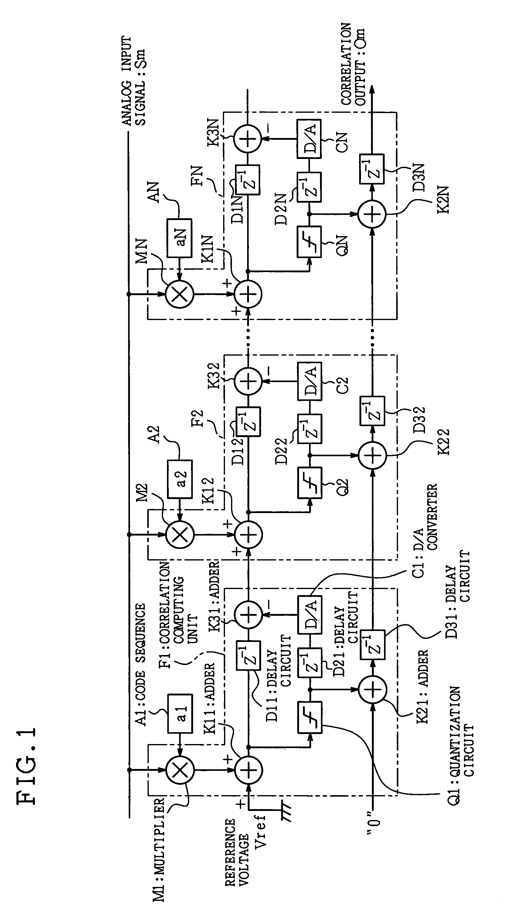
[0056]FIG. 2 is a block diagram showing an electric construction of a matched filter in accordance with Embodiment 2 of the present invention. The matched filter is similar to the FIR filter of FIG. 1. The corresponding members described in Embodiment 1 are indicated by the same reference numerals and the description thereof is omitted. It is noteworthy that an adder K3j-1 serving as a third adding means is functioned by an adder K1j serving as a first adding means. The analog adder K1j realized by an operational amplifier and the like is capable of mutually performing adding and subtracting on 3 or more inputs. The output (analog signal) from the D / A converter Cj−1 is subtracted by the adder K1j so as to obtain the analog residual signal.

[0057]Furthermore, the matched filter is used in the spread spectrum receiver to perform a reverse spread, so that the code sequence Aj serves as a...

embodiment 3

[0060]Referring to FIG. 3, the following explanation describes Embodiment 3 of the present invention.

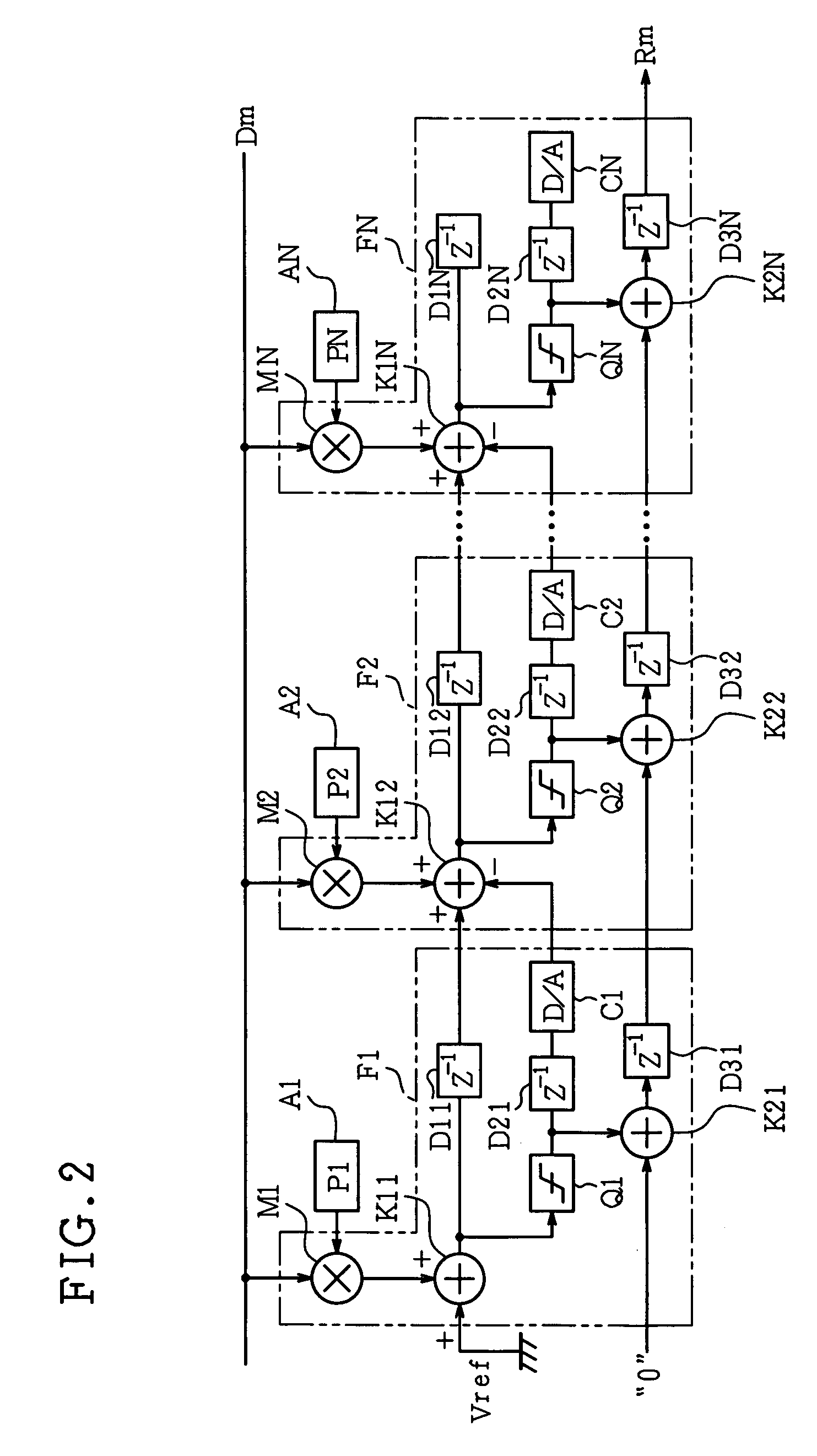
[0061]FIG. 3 is a block diagram showing an electric construction of a matched filter according to Embodiment 3 of the present invention. The matched filter is similar to that of FIG. 2. The corresponding members are indicated by the same reference numerals and the description thereof is omitted. In this matched filter, it is noteworthy that a quantization circuit Qi, a delay circuit D2i, a D / A converter Ci, and an adder K3i are omitted in some correlation computing unit Fi (i=2, 4, . . . , N−1). In FIG. 3, the above members are omitted for every other stage of the correlation computing unit Fj, namely, in N / 2 stages of the N stages of the correlation computing unit Fj.

[0062]In the correlation computing unit F1 in which the members are omitted, a multiplier Mi computes the partial correlation value, an adder K1i adds the partial correlation value to the analog residual signal from the...


PUM


Abstract

In a filter circuit of the present invention, a partial quantization value is computed by a quantization circuit according to a spread code and others in a unit at an arbitrary stage, where an integrating value is increased. The partial quantization value is successively added by an adder formed by a counter and is transmitted to a unit of the following stage. In an adder of the following stage, an analog residual is computed by subtracting an analog converted value of the partial quantization value, that is obtained by a D/A converter, from the integrating value so as to suppress an increase in the analog cumulative value. With this arrangement, the cumulative value is increased according to an increase in the number of taps, so that an analog adder can reduce power consumption, which is caused by expansion of a dynamic range at the following stage.

Description

FIELD OF THE INVENTION[0001]The present invention relates to a filter circuit which performs a sampling on a series of analog input signals, inputs them on a time series, and simultaneously multiplies a time-series analog sampling signal by a coefficient before computing, and particularly concerns a filter circuit which is suitably adopted as a matched filter and a band limitation filter of a receiver disposed in a radio using a spread spectrum method.BACKGROUND OF THE INVENTION[0002]Conventionally, a matched filter has been used as a reverse spread means of the spread spectrum receiver. FIG. 18 shows a construction example of a conventional N-type matched filter. In FIG. 18, dm and rm respectively represent a spread spectrum receive signal and a correlation signal, and pn represents a spread code of period N (n=0, 1, 2, . . . , N−1). Assuming that an interval length (chip interval length) of the spread code pn is Tc, the receive signal dm is subjected to a sampling with the same pe...

Claims


Application Information

Patent Timeline
Patent Type & Authority Patents(United States)
IPC IPC(8): H03H7/30H03H15/00H03M1/66H03H17/00H03H17/02H03H17/06H03M1/00H03M1/12H03M1/14H04B1/707H04B1/7093
CPCH03H15/00H03M1/147H03M1/002
Inventor HARA, KEITAIIZUKA, KUNIHIKO
Owner SHARP KK
Why Eureka
Try Eureka