Circuits and techniques for conditioning differential signals

a differential signal and circuit technology, applied in the field of circuitry and methods, can solve the problems of jitter of the output signal produced by the input buffer, erratic appearance, and inability to adapt to several drawbacks, and achieve the effect of increasing the range of common-mode voltages in which the input buffer can operate, increasing propagation delay, and increasing the range of common-mode voltages

Inactive Publication Date: 2006-01-10
ALTERA CORP
View PDF5 Cites 13 Cited by
  • Summary
  • Abstract
  • Description
  • Claims
  • Application Information

AI Technical Summary

Benefits of technology

[0007]As a result of this transformation, the common-mode of the conditioned input signal is expanded and shifted relative to the common-mode voltage originally associated with the signal. For example, if the common-mode voltage of the incoming differential signal ranges anywhere from 0 volts to 2.0 volts, the transformed common-mode voltage may result in ranging from 0.8 to 1.5 volts. Thus, when the input buffer receives the transformed differential signal, it sees a signal with a shifted common-mode range which advantageously puts the input buffer in a favorable common-mode mode of operation. Now that the input buffer receives this shifted differential signal, the input buffer does not experience substantial increases in propagation delay for a given common-mode voltage. Hence, the range of common-mode voltages in which the input buffer can operate is increased. That is, the input buffer is able to process a greater range of common-mode voltages because it does not receive common-mode voltages that would otherwise cause pronounced propagation delays. In addition, because occurrences of pronounced propagation delays are minimized, jitter tolerance is increased.
[0008]The feed-forward circuitry can be used in combination with a programmable amplifier that amplifies the magnitude of the differential amplitude voltage of the altered signal prior to being received by the input buffer. Amplifying the differential amplitude voltage puts the input buffer in an advantageous operating mode by enabling it to quickly detect low voltage signals that would not otherwise be readily detected. Thus, by amplifying the altered signal, the propagation delay is significantly reduced over the range of differential input voltage amplitude received by the input buffer. One advantage of amplifying the signal is that it reduces or eliminates data-dependent jitter caused by intersymbol interference.

Problems solved by technology

While multi-standard differential input buffers can handle two or more signaling standards, they can be susceptible to several drawbacks, especially when powered by a low voltage power supply.
One such drawback is signal jitter of the output signal produced by the input buffer.
Signal jitter causes a signal to appear erratic and random and it can create difficulties for other circuitry to process the signal (because the circuitry may not be able to tell if the signal is a logic LOW or HIGH).
Signal jitter can be caused by prolonged time delays in signal propagation through the buffer.
In general, all signals are subject to propagation delays when processed by an input buffer, but signals of certain voltages are processed much slower, resulting in prolonged propagation delays.
Sources of prolonged time delay include signals having certain ranges of common-mode voltage and relatively low differential amplitude voltage.
Certain ranges of common-mode voltage can result in pronounced propagation delays because multi-standard input buffers operating with low voltage power supply voltage (e.g., at about 1.5 volts or less) may not be able to quickly process signals operating within that particular range of common-mode voltages.
In addition, a relatively low differential amplitude voltage can cause propagation delays because the signal may be too weak to quickly drive the appropriate circuitry.
If the voltage is too low, problems associated with inter-signal interference can occur, which can cause data-dependent jitter.

Method used


Image

  • Circuits and techniques for conditioning differential signals
  • Circuits and techniques for conditioning differential signals
  • Circuits and techniques for conditioning differential signals

Examples


Embodiment Construction

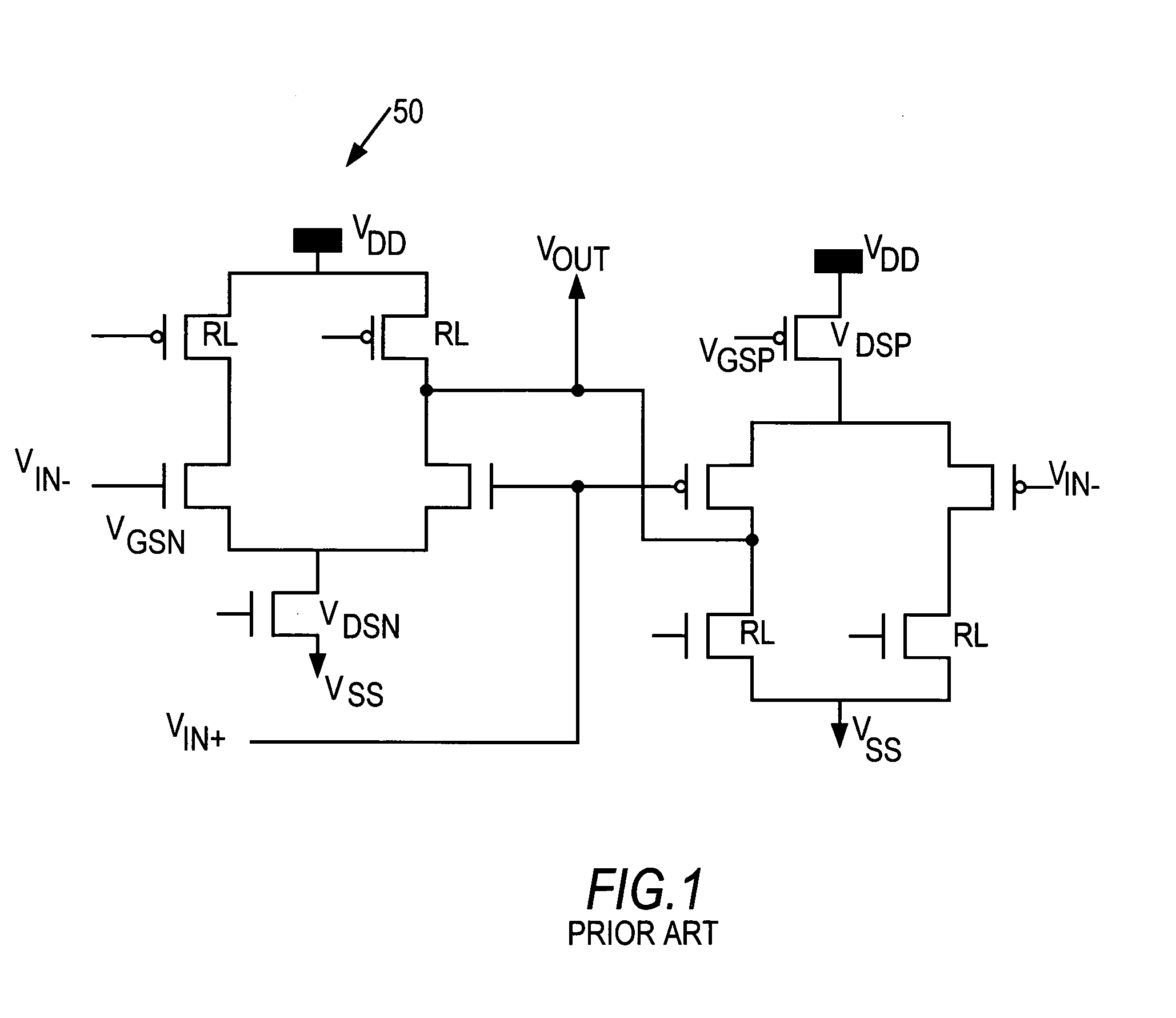
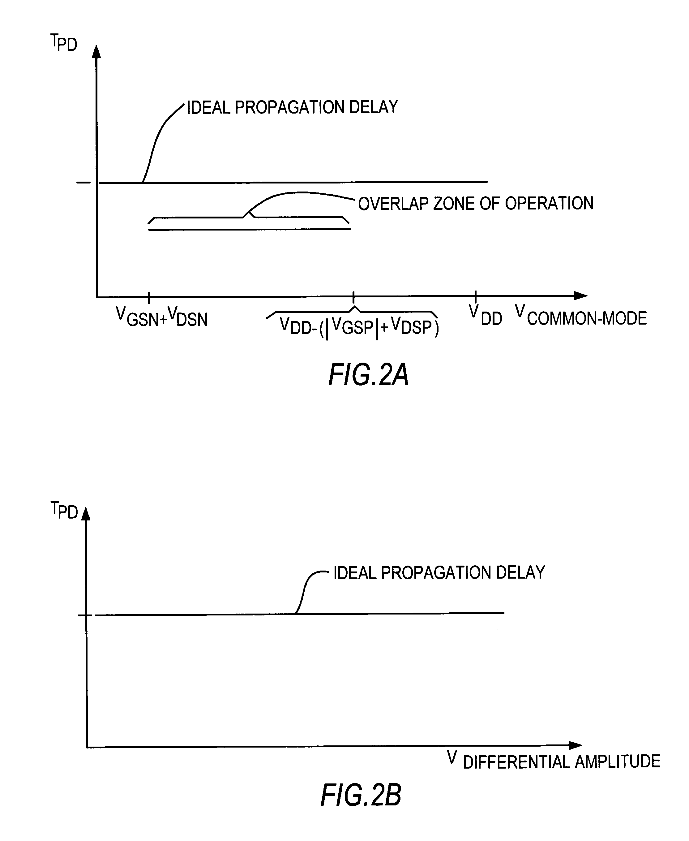
[0022]FIG. 1 shows a known multi-standard differential input buffer 50 that receives a differential input signal and produces a single output signal. In order for input buffer 50 to support multiple input standards, buffer 50 preferably operates over a wide range of common-mode voltage, while at the same time processing differential signals with a substantially constant propagation delay as a function of common-mode voltage. The common-mode in differential signaling is the DC level that should be midway between the two differential signals. The common-mode operational range of buffer 50 is generally defined by the saturation characteristics of the transistors. It is therefore preferable to maintain the transistors in saturation, otherwise when the transistors begin to fall out of saturation, propagation delays begin to increase.

[0023]In general, buffer 50 operates as follows. When the common-mode input voltage is less than combined gate-to-source voltage and drain-to-source voltage ...


PUM


Abstract

Circuitry is provided that conditions a differential input signal such that when the signal is received by a multi-standard differential input buffer, the buffer is able to process the conditioned signal without pronounced increases in propagation delay, thereby keeping signal jitter to a minimum. The circuitry further enables input buffers to operate according to desired operating parameters even when the supply voltage powering the input buffer is relatively low. The circuitry operates by shifting the common-mode voltage to a range that puts the input buffer in a favorable common-mode voltage range of operation. The circuitry may be coupled with a programmably controlled amplifier that amplifies the amplitude of the conditioned differential signal prior to being received by the input buffer. Amplifying the signal prevents problems typically associated with data-dependent jitter and intersymbol interference by boosting the voltage amplitude to a level that is readily processed by the input buffer.

Description

BACKGROUND OF THE INVENTION[0001]This invention relates to circuitry and methods that enhance the operation of input buffer circuitry, and more particularly to circuitry and methods that condition signals prior to being received by the input buffer circuitry.[0002]Input buffer circuitry is commonly used to receive signals and then transmit the received signals to other circuitry. Input buffer circuitry can be used to buffer, for example, circuitry (e.g., a programmable logic device) from input / output pins. Input buffers can be specifically designed to handle a particular type of signal (e.g., a differential signal) and can also be designed to operate according to a particular signaling standard such as Low Voltage Differential Signaling (“LVDS”). Other input buffers, such as multi-standard differential input buffers, are designed to support several signaling standards, including but not limited to, LVDS, Low Voltage Emitter Coupled Logic (“LVPECL”), LDT, and other standards used in ...

Claims


Application Information

Patent Timeline
Patent Type & Authority Patents(United States)
IPC IPC(8): H03F3/45
CPCH03F3/4521H03K19/003H03F3/45928H03F3/45475H03F2200/513H03F2203/45088H03F2203/45101H03F2203/45136H03F2203/45236H03F2203/45366H03F2203/45544H03F2203/45561H03F2203/45586H03F2203/45592H03F2203/45594H03F2203/45616
Inventor ZALIZNYAK, ARCHBEREZA, WILLIAMLUI, HENRYLEE, CHONGPATEL, RAKESH
Owner ALTERA CORP
Why Eureka
Try Eureka