Nanotube with at least a magnetic nanoparticle attached to the nanotube's exterior sidewall and electronic devices made thereof

Inactive Publication Date: 2006-01-17
CHEN YINGJIAN +1
View PDF5 Cites 50 Cited by
  • Summary
  • Abstract
  • Description
  • Claims
  • Application Information

AI Technical Summary

Benefits of technology

[0011]For long as-grown nanotubes, some further processing steps are required to tailor its length for device use. As a second step of this invention, a nano-grid technique is used to produce either nanotubes of the length 50–150 nm range suitable for FET gate fabrication, or of the length of microns suitable for interconnects. A grid made of lines of conductive metals (Cu, Au, W, Al, Cr, etc). The width of the lines defines the required length of the nanotubes. The nanotubes, which are dispensed onto the grid surface, are first made to align perpendicular to the grid lines by applying a large aligning field in the same direction. Alternatively, the same can be achie

Problems solved by technology

It is difficult to sort or position conventional nanotubes for the purpose of device fabrication, due

Method used


Image

  • Nanotube with at least a magnetic nanoparticle attached to the nanotube's exterior sidewall and electronic devices made thereof
  • Nanotube with at least a magnetic nanoparticle attached to the nanotube's exterior sidewall and electronic devices made thereof
  • Nanotube with at least a magnetic nanoparticle attached to the nanotube's exterior sidewall and electronic devices made thereof

Examples


Embodiment Construction

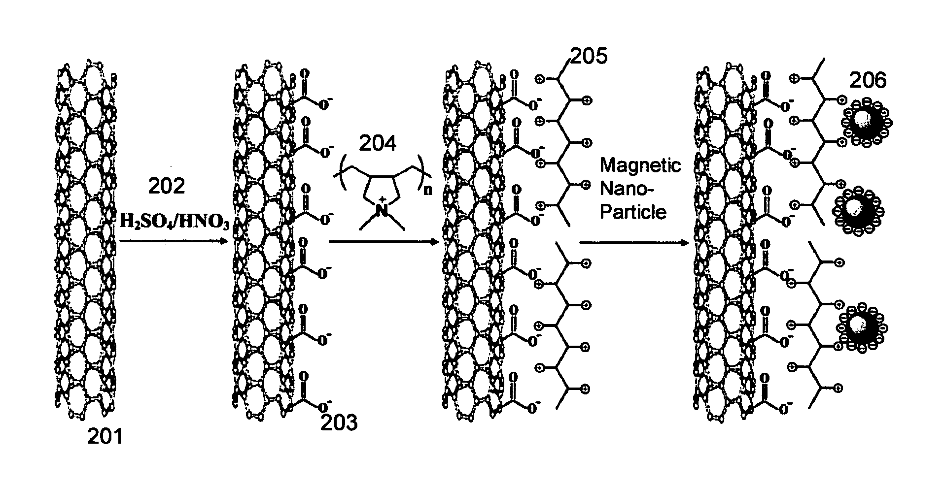
[0025]The purpose of present invention is providing enabling techniques of integrating novel nanotube elements into semiconductor devices, FET device in particular. This is done in a series of process steps, which consist of attaching magnetic nanoparticles to nanotubes, and tailoring the nanotubes to selected size (diameter and length), filtration of nanotube powders, preparing nanotube precursor in aqueous chemicals to form colloidal solutions of proper concentration, dispersing nanotube-containing solutions onto wafer surface, and finally positioning nanotubes at desired locations by magnetic means to complete nanotube device structure. The key to this invention is to provide miniature nanotubes with tangible physical properties, in this case, magnetic properties, so that they can be aligned, filtered, and precisely directed to desired locations for device application. Such processes enable nanotubes to be compatible with typical semiconductor wafer processing technologies.

[0026]...


PUM


Abstract

Present invention provides enabling methods of integrating novel nanotube elements into semiconductor devices, such as transistor containing electronic device. This is done in a series of process steps, which consist of attaching magnetic nanoparticles to nanotubes, tailoring magnetic nanotubes of selected size (diameter and length), filtration of nanotube to pre-determined sizes, preparing nanotube precursor in aqueous chemicals to form colloidal solutions of proper concentration, dispersing nanotube-containing solutions onto wafer surface, and finally positioning nanotubes at desired locations by magnetically assisted assembly to complete nanotube device structure. The key to this invention is to provide miniature nanotubes with tangible physical properties, in this case, magnetic properties, so that they can be aligned, filtered, and precisely directed to desired locations for device application. Such processes enable nanotubes to be compatible with typical semiconductor wafer processing technologies.

Description

BACKGROUND OF THE INVENTION[0001]1. Field of the Invention[0002]The present invention relates generally to the field of semiconductor devices. More particularly, to the application of carbon nanotube in field effect transistors (FET), and the manufacturing method of producing mass quantity of such transistors at wafer level, while achieving precision positioning of carbon nanotubes as gate channels and interconnects. This invention may also be used to fabricate magnetic random access memory devices.[0003]2. Relevant Background[0004]Carbon nanotube exhibits intriguing electronic properties that give rise to the possibility of being utilized in FETs. As a result of different quantum states depending on the size and chiral structure, nanotubes can behave as semiconductor whose conductivity may be changed by a factor of one million or more, comparable to the change in silicon FET. Because of its tiny size, nanotube used as the gate of FET gives rise to significantly lower power consumpt...

Claims


Application Information

Patent Timeline
IPC IPC(8): H01L29/76H01L31/062H01L31/113H01L29/94H01L31/119
CPCB82Y10/00B82Y25/00B82Y30/00B82Y40/00H01F1/0054G01N27/4146C01B31/0253Y10S977/936Y10S977/745C01B32/168
Inventor CHEN, YINGJIANDANG, XIAOZHONG
Owner CHEN YINGJIAN
Why Eureka
Try Eureka