Image pickup system with MOS sensors and microlenses

a pickup system and microlense technology, applied in the field of image pickup systems, can solve the problems of difficult condense light in the photoelectric transfer region, low efficiency, and low efficiency of image pickup, and achieve the effects of high density integration, good image pickup characteristics, and rapid operation

Inactive Publication Date: 2006-01-17
SK HYNIX INC
View PDF3 Cites 7 Cited by
  • Summary
  • Abstract
  • Description
  • Claims
  • Application Information

AI Technical Summary

Benefits of technology

[0018]It is therefore an object of the present invention to eliminate the aforementioned problems and to provide an image pickup system capable of obtaining good image pickup characteristics and of achieving high density integration and rapid operations.

Problems solved by technology

For that reason, there is a problem in that the high density integration and accelerating of the peripheral circuits have not been realized.
When the operation of the peripheral circuits is accelerated or when circuits (including the MOS sensor) formed on the same substrate are formed of a multi layer metallization in order to facilitate design, it is difficult to condense light in the photoelectric transfer region, so that image pickup characteristics deteriorate.
However, in the image pickup system shown in FIG. 17, the distance between the photoelectric transfer layer 27a and the microlens 32 is longer than the focal length of the microlens 32, so that the picture light signal 40 is difficult to form an image on the photoelectric transfer layer 27a, thereby deteriorating image pickup characteristics.

Method used


Image

  • Image pickup system with MOS sensors and microlenses
  • Image pickup system with MOS sensors and microlenses
  • Image pickup system with MOS sensors and microlenses

Examples


first preferred embodiment

(First Preferred Embodiment)

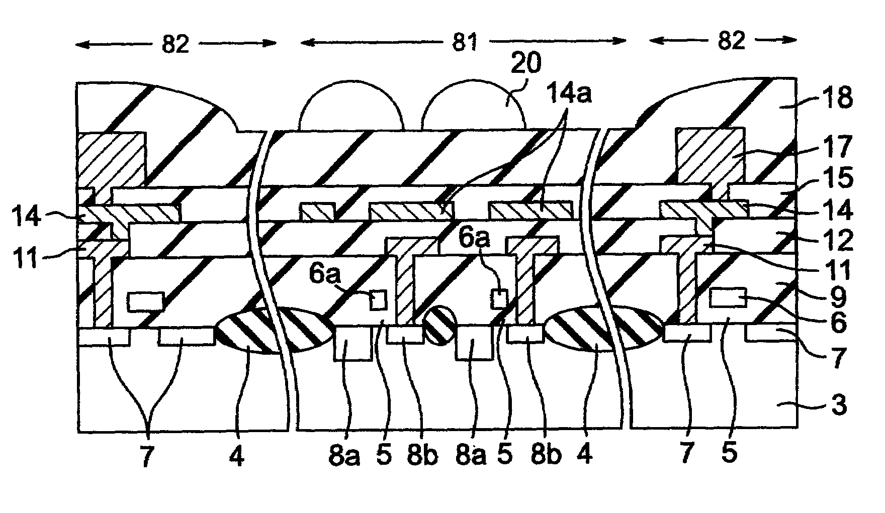
[0044]Referring to FIGS. 1 through 6, the first preferred embodiment of an image pickup system according to the present invention will be described below. FIG. 1 is a sectional view showing the construction of an image pickup system according to the present invention, and FIGS. 2 through 6 are sectional views showing a process for fabricating the image pickup system in this preferred embodiment.

[0045]In the image pickup system in this preferred embodiment, MOS sensors and their peripheral circuits are formed on the same chip. That is, as shown in FIG. 1, in the image pickup region 81 of a semiconductor substrate 3 on which MOS transistors are to be formed, there are formed photoelectric transfer layers 8a for converting picture light signals into picture electric signals, and diffusion layers 8b. On the semiconductor substrate between the photoelectric transfer layers 8a and the diffusion layers 8b, gate electrodes 6a are formed via a gate insulating film...

second preferred embodiment

(Second Preferred Embodiment)

[0056]FIG. 7 shows the construction of the second preferred embodiment of an image pickup system according to the present invention. In the image pickup system in this second preferred embodiment, each the second wiring layers 14 in the peripheral circuit region 82 of the image pickup system in the first preferred embodiment shown in FIG. 1 is replaced with a double-layer structure of a wiring layer 141 and a wiring layer 142, and the thickness of the wiring structure is greater than that in the first preferred embodiment. Furthermore, the wiring layers 141 and shading films 14a are formed in the same layer.

[0057]Thus, in this preferred embodiment, the second wiring layer 14 in the peripheral circuit region 82 is thicker than that in the first preferred embodiment, so that it is possible to carry out a more rapid operation. Furthermore, similar to the first preferred embodiment, the image pickup system in the second preferred embodiment can also obtain g...

third preferred embodiment

(Third Preferred Embodiment)

[0058]Referring to FIGS. 8 through 14, the third preferred embodiment of an image pickup system according to the present invention will be described below. FIG. 8 is a sectional view showing the construction of an image pickup system according to the present invention, and FIGS. 9 through 14 are sectional views showing a process for fabricating the image pickup system in this preferred embodiment.

[0059]In the image pickup system in this preferred embodiment, the insulating film 18 in the image pickup region 81 of the image pickup system in the second preferred embodiment shown in FIG. 7 is removed, and the flattened insulating film 15 is thinned. In addition, color filter (not shown) and microlenses 20 are formed on the thinned flattened insulating film 15.

[0060]Furthermore, in this preferred embodiment, the uppermost insulating film 18 is flattened. In the third preferred embodiment, as compared with the second preferred embodiment, the distance between ...


PUM


Abstract

The image pickup system includes: MOS sensors arranged in an image pickup region of a semiconductor substrate in the form of a matrix and having photoelectric transfer layers; a peripheral circuit part formed in a region of the semiconductor substrate except for the image pickup region and having a driving circuit for driving the MOS sensors and a signal processing circuit for processing output signals from the MOS sensors; and microlenses, formed on the photoelectric transfer layers via a first insulating film, for condensing picture signals on the photoelectric transfer layers, wherein the driving circuit and the signal processing circuit in the peripheral circuit part are covered by a second insulating film, and the distance between the surface of the first insulating film and the semiconductor substrate is shorter than the distance between the surface of a second insulating film and the semiconductor substrate.

Description

CROSS REFERENCE TO RELATED APPLICATION[0001]This application claims benefit of priority under 35USC § 119 to Japanese Patent Application No. 2000-110915, filed on Apr. 12, 2000, the contents of which are incorporated by reference herein.BACKGROUND OF THE INVENTION[0002]1. Field of the Invention[0003]The present invention relates generally to an image pickup system having a solid state image sensor device.[0004]2. Description of Related Art[0005]In recent years, MOS solid stage image pickup elements are widely noticed since there are advantages in that required voltages and costs are low and only one power supply is required.[0006]Since a signal processing circuit for processing signals, which are outputted from a solid stage image sensor device having MOS solid state image pickup elements, comprises MOS transistors, the solid state image sensor device can be fabricated in the same fabricating process as a process for fabricating the signal processing circuit and can be formed on the...

Claims


Application Information

Patent Timeline
Patent Type & Authority Patents(United States)
IPC IPC(8): H04N5/335H01L27/146H01L31/0232H01L31/10H04N5/369H04N5/374H04N5/376
CPCH01L27/14609H01L27/14621H04N5/335H01L27/14692H01L27/14627H04N25/00H01L27/14
Inventor INOUE, IKUKO
Owner SK HYNIX INC
Why Eureka
Try Eureka