Magnetoresistive element and magnetic memory device

a magnetic memory device and magnetoresistance technology, applied in the field of magnetoresistance elements and magnetic memory devices, can solve the problems of reducing mr change, reducing mr change, and gradually decreasing output, so as to reduce mr change

Inactive Publication Date: 2006-01-17
TOSHIBA MEMORY CORP
View PDF41 Cites 29 Cited by
  • Summary
  • Abstract
  • Description
  • Claims
  • Application Information

AI Technical Summary

Benefits of technology

[0011]An object of the present invention is to provide a magnetoresistive element of a tunnel junction type and a magnetic memory device in that reduction in the MR change can be made low even when an applied voltage is increased to obtain required output voltage, that have no problem that an output is gradually decreased owing to rotation of a part of magnetic moments in the magnetization pinned layer by repeated writing, and in that an reversal magnetic field for reversing the magnetic moments in the ferromagnetic layer can be freely designed.
[0012]Another object of the present invention is to provide a magnetoresistive element of a tunnel junction type and a magnetic memory device that can suppress increase in reversal magnetic field for reversing the magnetization of the magnetic recording layer accompanying scaling down of memory cells.

Problems solved by technology

However, there is a problem that the magnetoresistance (MR) change is considerably decreased in the ferromagnetic single tunnel junction element, when a voltage to be applied is increased to obtain required output voltage (Phys. Rev. Lett. 74, 3273 (1995)).
However, such an element also has a similar problem that the MR change is considerably decreased when an applied voltage is increased to obtain required output voltage.
Moreover, as the ferromagnetic double tunnel junction element of the above structure has no ferromagnetic layer pinned with an antiferromagnetic layer, there is a problem that the output is gradually decreased owing to rotation of a part of magnetic moments in a magnetization pinned layer by performing writing several times when it is used for MRAM and the like.
However, as the element has no ferromagnetic layer pinned with an antiferromagnetic layer, there is a problem that the output is gradually decreased owing to rotation of a part of magnetic moments in a magnetization pinned layer by performing writing several times when it is used for MRAM and the like.
As a ferromagnetic double tunnel junction element using a ferromagnetic layer consisting of a continuous film (Appl. Phys. Lett. 73(19), 2829(1998)) has a ferromagnetic layer consisting of a single layer film of, for example, Co, Ni80Fe20 between dielectric layers, there are problems that a reversal magnetic field for reversing the magnetic moment may not be freely designed, and that coercive force of the ferromagnetic layer may be increased when the material such as Co is processed.
Thus, power consumption is increased for writing as memory capacity of the MRAM is increased.
For example, in an MRAM device with a high density of 1 Gb or more, there may be caused a problem that the wires melt owing to increased current density for writing in the wires.
However, the method for performing magnetization reversal by injection of the spin current causes increase in current density in the TMR element, which leads to destruction of a tunnel insulator.
Moreover, there have been no proposals for an element structure suitable for spin injection.

Method used


Image

  • Magnetoresistive element and magnetic memory device
  • Magnetoresistive element and magnetic memory device
  • Magnetoresistive element and magnetic memory device

Examples


embodiment 1

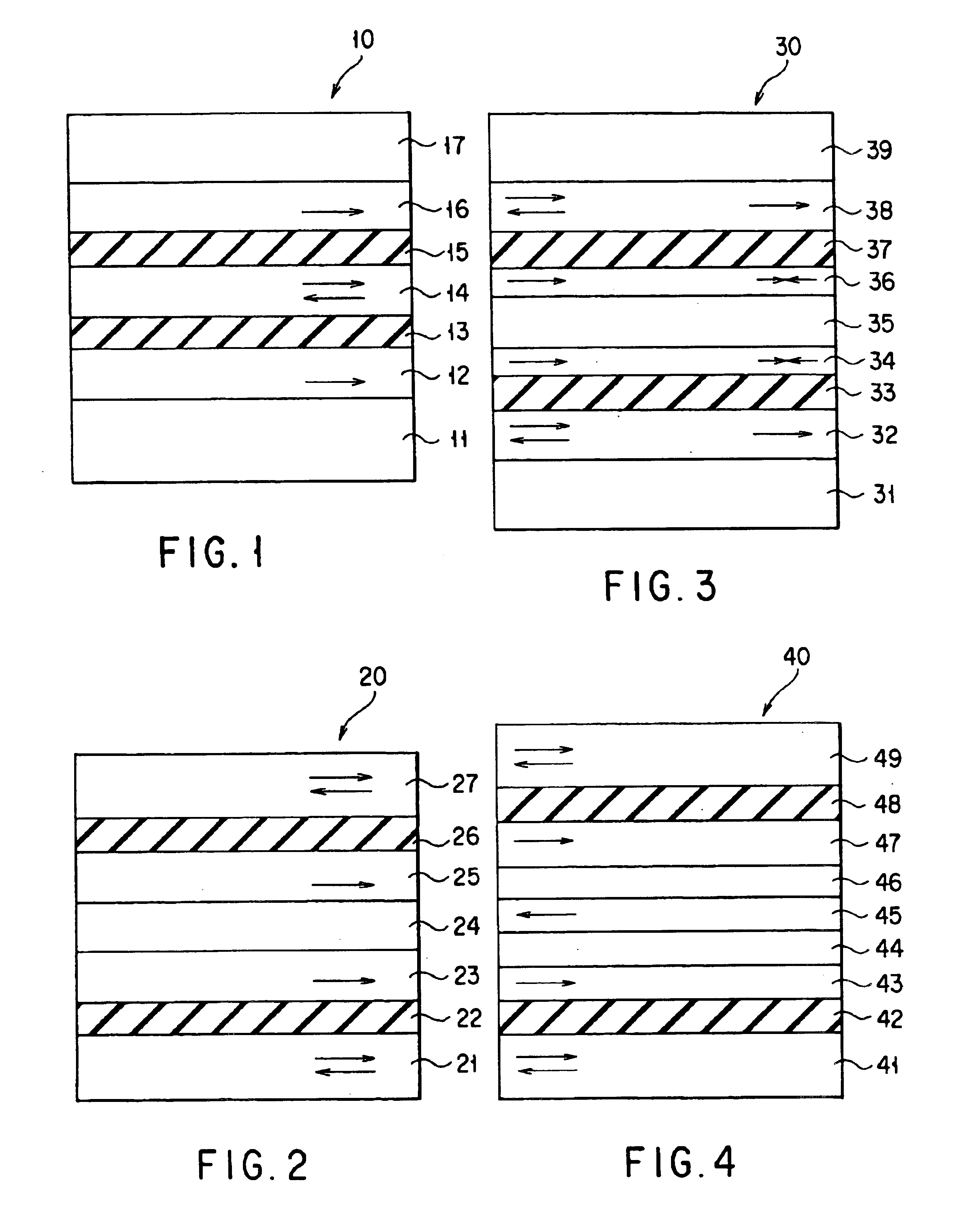
[0133]An embodiment, where two kinds of ferromagnetic double tunnel junction elements (sample A, and B) with the structure shown in FIG. 1 were formed on a Si / SiO2 substrate or SiO2 substrate, will be described below.

[0134]The sample A has a structure sequentially stacked with a TaN underlayer, a first antiferromagnetic layer of a two-layered film of Fe—Mn / Ni—Mn, a first ferromagnetic layer of CoFe, a first dielectric layer of Al2O3, a second ferromagnetic layer of Co9Fe, a second dielectric layer of Al2O3, a third ferromagnetic layer of CoFe, a second antiferromagnetic layer of a two-layered film of Ni—Fe / Fe—Mn, and a protective layer of Ta.

[0135]The sample B has a structure sequentially stacked with a TaN underlayer, a first antiferromagnetic layer of Ir—Mn, a first ferromagnetic layer of Co—Fe, a first dielectric layer of Al2O3, a second ferromagnetic layer of a three-layered film of CoFe / Ni—Fe / CoFe, a second dielectric layer of Al2O3, a third ferromagnetic layer of CoFe, a secon...

embodiment 2

[0150]An embodiment, where two kinds of ferromagnetic double tunnel junction elements (sample A2, and B2) with the structure shown in FIG. 2 were formed on a Si / SiO2 substrate or SiO2 substrate, will be described below.

[0151]The sample A2 has a structure sequentially stacked with a TaN underlayer, a first ferromagnetic layer of a two-layered film of Ni—Fe / CoFe, a first dielectric layer of Al2O3, a second ferromagnetic layer of CoFe, an antiferromagnetic layer of Ir—Mn, a third ferromagnetic layer of CoFe, a second dielectric layer of Al2O3, a fourth ferromagnetic layer of a two-layered film of CoFe / Ni—Fe, and a protective layer of Ta.

[0152]The sample B2 has a structure sequentially stacked with a TaN underlayer, a first ferromagnetic layer of a three-layered film of Ni—Fe / Ru / CoFe, a first dielectric layer of Al2O3, a second ferromagnetic layer of a two-layered film of CoFe / Ni—Fe, a first antiferromagnetic layer of Fe—Mn, a third ferromagnetic layer of a two-stacked film of Ni—Fe / CoF...

embodiment 3

[0167]An embodiment, where two kinds of ferromagnetic double tunnel junction elements (sample A3, and B3) with the structure shown in FIG. 3 were formed on a Si / SiO2 substrate or SiO2 substrate, will be described below.

[0168]The sample A3 has a structure sequentially stacked with a TaN underlayer, a first antiferromagnetic layer of Ir—Mn, a first ferromagnetic layer of Co—Fe, a first dielectric layer of Al2O3, a second ferromagnetic layer of Co—Fe—Ni, a second antiferromagnetic layer of Fe—Mn, a third ferromagnetic layer of Co—Fe—Ni, a second dielectric layer of Al2O3, a fourth ferromagnetic layer of Co—Fe, an third antiferromagnetic layer of Ir—Mn, and a protective layer of Ta.

[0169]The sample B3 has a structure sequentially stacked with a TaN underlayer, a first antiferromagnetic layer of Ir—Mn, a first ferromagnetic layer of a three-layered film of Co—Fe / Ru / Co—Fe, a first dielectric layer of Al2O3, a second ferromagnetic layer of a two-layered film of CoFe / Ni—Fe, a second antifer...


PUM

PropertyMeasurementUnit
thicknessaaaaaaaaaa
thicknessaaaaaaaaaa
thicknessaaaaaaaaaa

Abstract

A magnetoresistive element has a ferromagnetic double tunnel junction having a stacked structure of a first antiferromagnetic layer / a first ferromagnetic layer / a first dielectric layer / a second ferromagnetic layer / a second dielectric layer / a third ferromagnetic layer / a second antiferromagnetic layer. The second ferromagnetic layer that is a free layer consists of a Co-based alloy or a three-layered film of a Co-based alloy / a Ni—Fe alloy / a Co-based alloy. A tunnel current is flowed between the first ferromagnetic layer and the third ferromagnetic layer.

Description

CROSS-REFERENCE TO RELATED APPLICATIONS[0001]This is a divisional application of U.S. application Ser. No. 10 / 443,830, filed on May 23, 2003 now U.S. Pat. No. 6,751,074, which is a divisional application of U.S. application Ser. No. 09 / 662,117, filed on Sep. 14, 2000 now U.S. Pat. No. 6,611,405.[0002]This application is based upon and claims the benefit of priority from the prior Japanese Patent Applications No. 11-262327, filed Sep. 16, 1999; No. 11-263741, filed Sep. 17, 1999; No. 2000-265663, filed Sep. 1, 2000; and No. 2000-265664, filed Sep. 1, 2000, the entire contents of which are incorporated herein by reference.BACKGROUND OF THE INVENTION[0003]The present invention relates to a magnetoresistive element having ferromagnetic double tunnel junction, and, a magnetic memory device using the same.[0004]The magnetoresistance effect is a phenomenon that electrical resistance changes when a magnetic field is applied to a ferromagnetic material. As the magnetoresistive element (MR el...

Claims


Application Information

Patent Timeline
Patent Type & Authority Patents(United States)
IPC IPC(8): G11B5/39G11C11/14G11C11/15G01R33/09G11C11/16H01F10/32H01L21/8246H01L27/22H01L43/08
CPCB82Y10/00G01R33/093G11B5/3903G11B5/3909G11C11/15G11C11/16H01F10/3254H01F10/3263H01F10/3281H01L27/224H01L27/228H01L43/08B82Y25/00Y10T428/1121H01F10/3272Y10T428/115H10B61/10H10B61/22H10N50/10
Inventor INOMATA, KOICHIRONAKAJIMA, KENTAROSAITO, YOSHIAKISAGOI, MASAYUKIKISHI, TATSUYA
Owner TOSHIBA MEMORY CORP
Why Eureka
Try Eureka