Method of manufacturing semiconductor device having damascene interconnection

a technology of damascene and semiconductors, which is applied in the direction of semiconductor devices, basic electric elements, electrical appliances, etc., can solve the problems of large load on the cmp, erosion of fine patterns, and large fine patterns, so as to reduce the quality of plating films, suppress the protrusion of fine patterns, and improve the effect of quality

Active Publication Date: 2006-01-24
RENESAS ELECTRONICS CORP
View PDF7 Cites 2 Cited by
  • Summary
  • Abstract
  • Description
  • Claims
  • Application Information

AI Technical Summary

Benefits of technology

[0012]The present invention was devised considering the above-described problems, and the major object of the present invention is to solve the problems of protrusions on fine pattern portions in the Cu-plating process in the damascene process, without lowering the fine-pattern filling properties, the plating film quality, and the reliability of devices. As a result, there is provided a method for manufacturing a semiconductor device that can reduce CMP costs, suppress erosion 13 or dishing 14 occurring during CMP, and form the device having a uniform wiring height.
[0016]The present inventors examined the method of electroplating having a backward current step, and found that the application time of the backward current and the optimization of the current values were very important; and that the forward current values after applying the backward current had to be optimized. Furthermore, the present inventors found that the more the number of steps applying backward current, the lower the quality of the plating film. In other words, a plating film of a high quality can be obtained, the protrusions on fine patterns can be suppressed, the time required to completely remove excessive Cu by CMP can be shortened, and CMP costs can be lowered by performing only one step of applying backward current, and by performing electroplating under conditions favorable to each of the above-described steps. Moreover, since erosion or dishing occurring when excessive Cu of CMP is completely removed can be suppressed, the Cu damascene wiring of high reliability with a uniform wiring height can be provided.

Problems solved by technology

However, in the plating method having bottom-up properties, protrusions occur on the fine patterns.
However, since these methods cannot solve the problem of protrusions on fine patterns, erosion 13 and dishing 14 after CMP are unavoidable.
Although U.S. Pat. No. 6,107,186 discloses that flat CMP can be performed by protruding the plating films of high pattern densities, the load to the CMP is large, and increase in CMP costs cannot be avoided.
In this method also, the load to the CMP is large, and increase in CMP costs cannot be avoided, as in the above-described U.S. Pat. No. 6,107,186.
The patent also discloses that the repetitive applications of polarity-inversion pulses are effective; however, the effect on the reliability of the devices is not described.

Method used


Image

  • Method of manufacturing semiconductor device having damascene interconnection
  • Method of manufacturing semiconductor device having damascene interconnection
  • Method of manufacturing semiconductor device having damascene interconnection

Examples


example

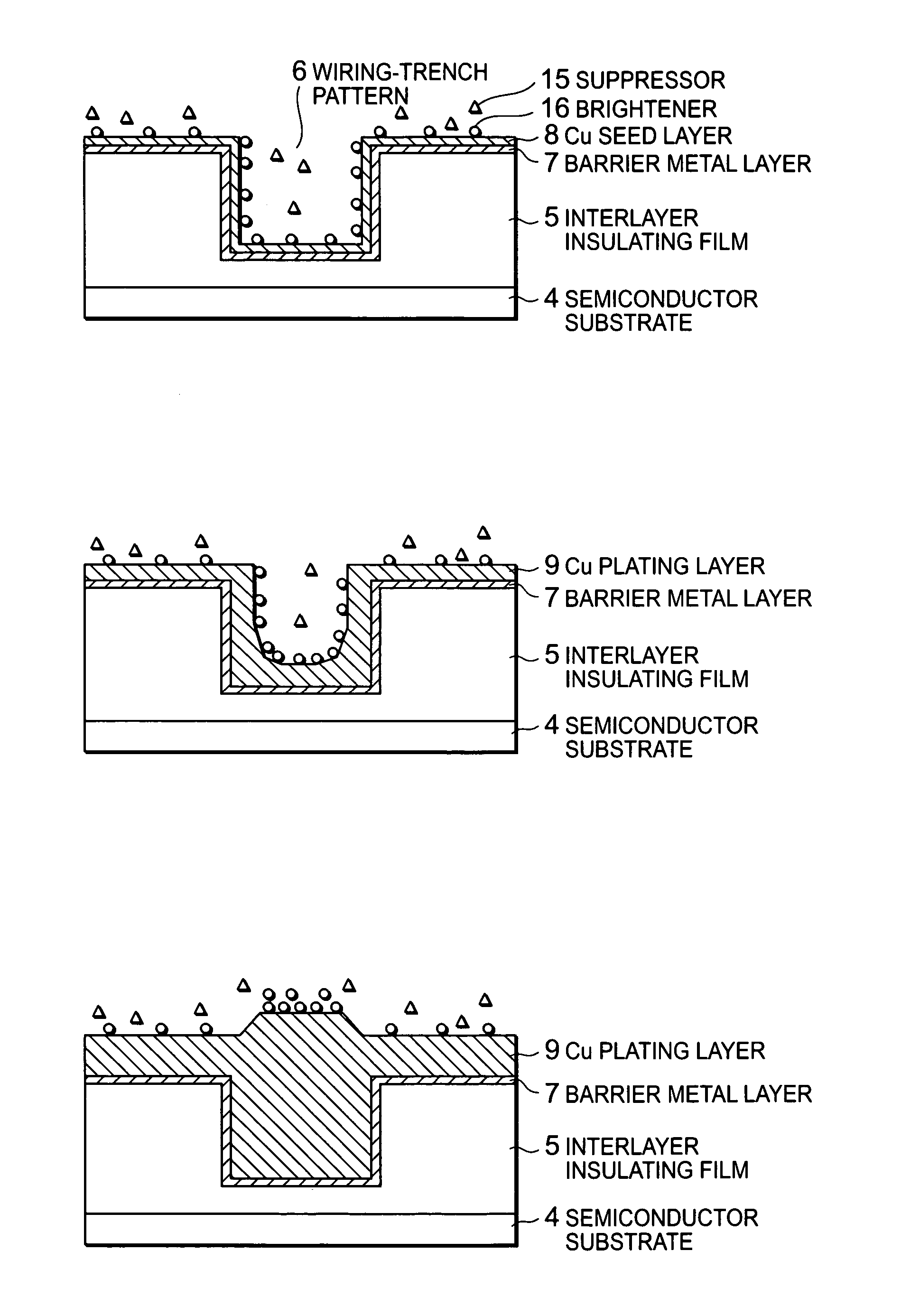
[0048]First, the damascene process according to the Example of the present invention will be described referring to FIG. 4. FIG. 4 is a sectional process diagram showing the procedures of the Damascene process whereto the current steps on the Cu plating of the present invention are applied.

[0049]First, as FIG. 4 (a) shows, an etching-stop film 10 and an interlayer insulating film 5 are sequentially formed in thickness of 50 nm and 30 nm, respectively, on a semiconductor substrate 4 using the well-known CVD method, plasma CVD method, or the like. Thereafter, an antireflective film 11 of a thickness of about 50 nm for suppressing the reflection of exposure light is deposited on the interlayer insulating film 5, and then a chemical-amplification-type resist of a thickness of about 500 nm for forming wiring-trench patterns 6 are applied to the antireflective film 11, and exposure and development are performed using KrF photolithography to form a resist pattern 12.

[0050]Next, as FIG. 4 (...


PUM

PropertyMeasurementUnit
currentaaaaaaaaaa
currentaaaaaaaaaa
currentaaaaaaaaaa

Abstract

In copper plating using a damascene method, in order to prevent cost rise, dishing, erosion and the like due to the protrusion of plating on the dense wiring area to increase the time for CMP polishing, the copper plating is performed so that the current step of the copper plating has only one step for flowing current in the direction opposite to the direction of growing the plating as shown in FIG. 1. In this time, this opposite direction current step is performed under the condition of a current-time product within a range between 1.0 and 120 mA×sec / cm2.

Description

BACKGROUND OF THE INVENTION[0001]1. Field of the Invention[0002]The present invention relates to a method of manufacturing a semiconductor device, and specifically to a method of manufacturing a semiconductor device that forms wirings of a uniform height after polishing in a damascene wiring process using a plating method.[0003]2. Description of the Related Art[0004]In recent years, the miniaturization of wirings and the production of multi-layer wiring have been progressed accompanying the higher integration of semiconductor devices and the size reduction of semiconductor chips, and as a method for forming a multi-layer wiring structure, there has generally been used a process known as the damascene process, wherein Cu, which is a wiring material, is simultaneously or sequentially buried in via holes and wiring-trench patterns through a Cu seed layer using an electroplating method, and planarized using CMP (chemical mechanical polishing) method to form wirings.[0005]The generally u...

Claims


Application Information

Patent Timeline
Patent Type & Authority Patents(United States)
IPC IPC(8): H01L21/44C25D7/12H01L21/288H01L21/3205H01L21/768
CPCH01L21/76877H01L21/2885
Inventor ARITA, KOJIMIKAGI, KAORUKITAO, RYOHEI
Owner RENESAS ELECTRONICS CORP
Why Eureka
Try Eureka