Non-quasistatic phase lock loop frequency divider circuit

a phase lock loop and frequency divider technology, applied in the field of phase lock loop circuit and frequency division method, can solve problems such as large signal voltage at the gates, and achieve the effect of easy operation

Active Publication Date: 2006-01-24
GULA CONSULTING LLC
View PDF8 Cites 8 Cited by
  • Summary
  • Abstract
  • Description
  • Claims
  • Application Information

AI Technical Summary

Problems solved by technology

Capacitive loading effects of the phase detector transistor gates are absorbed in the capacitance of the antenna tuned-circuit resulting in a large signal voltage at the gates.

Method used


Image

  • Non-quasistatic phase lock loop frequency divider circuit
  • Non-quasistatic phase lock loop frequency divider circuit
  • Non-quasistatic phase lock loop frequency divider circuit

Examples


first embodiment

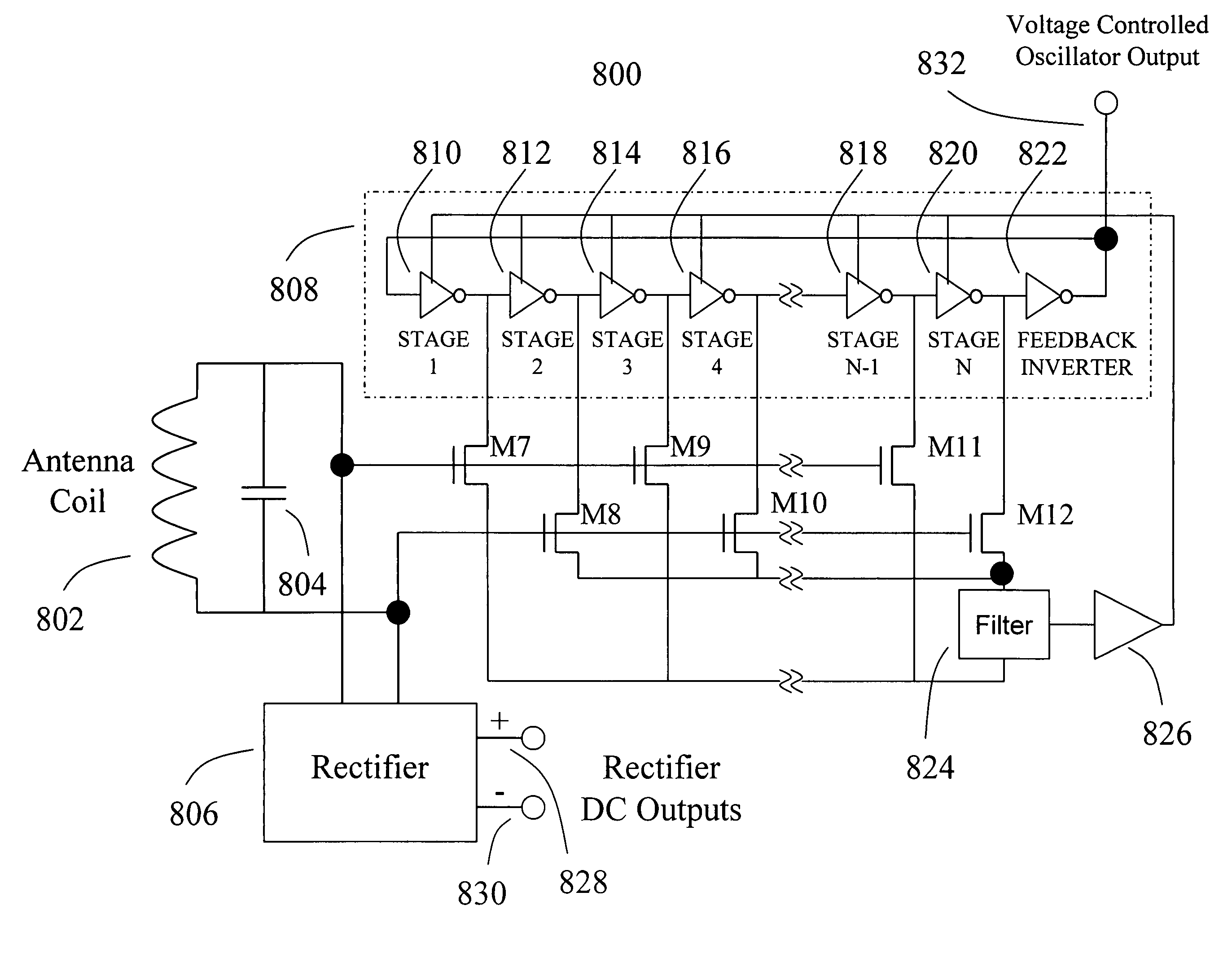
[0031]Referring now to FIG. 5 a phase lock loop frequency divider 500 according to the present invention includes first and second input terminals for receiving a differential input signal from antenna coil 502 and an output terminal 532 for providing a synchronous output signal, which is generated by voltage controlled oscillator 508. A capacitor 504 is coupled between the first and second input terminals. The voltage controlled oscillator 508 comprises delay stages 510, 512, 514, 516, 518 and 520, as well as feedback inverter stage 522. The inverting stage 522 may be included as part of stage 520 depending on the implementation of stage 520. The delay stages include an delay control input fed by loop amplifier 526. The voltage controlled oscillator 508 implements a ring oscillator. Each delay stage in the voltage-controlled oscillator provides time delay and phase inversion of the pulse signal passing through the oscillator loop. The feedback inverter 522 guarantees that the total...

second embodiment

[0042]Referring to FIG. 10, a delay circuit 1000 to be used in the voltage-controlled oscillators 508 or 808 comprises PMOS transistors M105, M106, M107 and M108. Transistor M105 has its source connected to the positive power supply its gate to the delay stage input 1002 and its drain to the gate of transistor M108. Transistor M106 has its source connected to the gate of transistor M108, its gate to delay control input 1006 and its drain connected to power supply ground. Transistor M108 has its source connected to delay stage output 1004, its gate to the drain of M105 and its drain connected to power supply ground. Transistor M107 has its source connected to positive power supply, its gate connected to a bias voltage 1008 and its drain connected to stage delay output 1004. Transistors M105 and M106 operate as in previously described delay cell 900. Transistors M107 and M108 operate as a voltage level shifter. The level shifter improves signal compatibility between oscillator delay s...

third embodiment

[0043]Referring to FIG. 11, a delay circuit 1100 to be used in the voltage-controlled oscillators 508 or 808 comprises PMOS transistors M114, M115, M116, M117 and M118. Transistor M114 has its source connected to the positive power supply, its gate to the delay stage input 1102 and its drain to the sources of transistors M115 and M116. M115 and M116 are configured as a differential amplifier with their gates connected to the positive input 1104 and negative input 1106, respectively and their drains connected to the negative output 1110 and positive output 1108, respectively. Load transistors M116 and M118 have their drains connected to the power supply ground. M116 and M118 are constant-current source connected with their gates connected to their associated drains. The drain of M116 is connected to the negative output 1110 and the drain of M118 is connected the positive output 1108. Change in the voltage at the delay control input 1102 causes a change in available current to be swit...


PUM


Abstract

A non-quasistatic MOS frequency divider circuit uses a phase lock loop configuration including an antenna coil to induce a differential input signal, an antenna resonating capacitor, a rectifier, a voltage controlled ring oscillator, a phase detector and a loop filter. All transistors used are organic MOS devices of PMOS, NMOS or both PMOS and NMOS varieties. The voltage-controlled oscillator includes a multiple delay stage ring oscillator. The phase detector includes transistors connected as sampling switches to sample the individual oscillator stage voltages into the loop filter. The sampling transistors have gates connected to the coil. The loop filter provides a substantially direct current to a loop amplifier and then to the voltage controlled oscillator delay control input. This configuration results in the voltage controlled oscillator frequency being synchronous to—and at a sub-multiple of the antenna signal frequency. The sampling transistor gates are all connected to the coil and thereby become part of the capacitance of the radio frequency parallel resonant network. The transistor gates are then efficiently switched at the rate of the radio frequency signal with no delay relative to the coil voltage. Operation of the phase detector organic transistors is based on non-quasistatic behavior of the transistor. Non-quasistatic operation results in phase detection at a frequency much higher than the quasistatic limit of transistor unity gain bandwidth.

Description

[0001]The present application is related to and claims priority from U.S. Provisional Application Ser. Nos. 60 / 536,603, filed Jan. 15, 2004, entitled “Circuitry for the Design of RFID Tags in Polymer Electronic Processes”, 60 / 539,611, filed Jan. 27, 2004, entitled, “RFID Organic Process Methods”, 60 / 539,612, filed Jan. 27, 2004, entitled, “RFID Organic Circuit Designs”, and 60 / 539,610, filed Jan. 27, 2004, entitled, “RFID Organic Flexographic Printline Method”. The disclosures of all four provisional applications are herein specifically incorporated in their entirety by this reference.BACKGROUND OF THE INVENTION[0002]1. Field of the Invention[0003]The invention relates to organic transistors, and, more particularly, to a phase lock loop circuit and frequency division method suitable for use given the performance constraints of organic transistors.[0004]2. Description of the Related Art[0005]Organic MOS transistors are similar to silicon metal-oxide-semiconductor transistors in opera...

Claims


Application Information

Patent Timeline
Patent Type & Authority Patents(United States)
IPC IPC(8): H03L7/06H03K3/03H03L7/091H03L7/099
CPCH03K3/0315H03L7/0995H03L7/091
Inventor DIMMLER, KLAUSROTZOLL, ROBERT R.
Owner GULA CONSULTING LLC
Why Eureka
Try Eureka