Screen print under-bump metalization (UBM) to produce low cost flip chip substrate

a flip chip substrate and metalization technology, applied in the field of integrated circuit fabrication and the formation of interconnect pads, can solve the problems of increasing the number of interconnect pads on the circuit chips, increasing the cost of the process of forming interconnect pads, and increasing the complexity of the integrated circuit industry. , to achieve the effect of reducing the production time of integrated circuits, reducing processing steps, and reducing cos

Inactive Publication Date: 2006-01-31
KULICKE & SOFFA IND INC
View PDF13 Cites 48 Cited by
  • Summary
  • Abstract
  • Description
  • Claims
  • Application Information

AI Technical Summary

Benefits of technology

[0005]The present invention pertains to a method of forming an integrated circuit and specifically to the formation of interconnect pads on the integrated circuit. Embodiments of the present invention provide a method of screen printing layers of an interconnect pad that does not engender the problems described above. Embodiments of the invention provide for relatively fewer processing steps to form the interconnect pad and the steps are relatively less costly than known methods. Accordingly, embodiments of the present invention may be characterized as lowering the production time of integrated circuits while at the same time reducing the cost of production.

Problems solved by technology

The semiconductor industry continues to produce integrated circuits (ICs) of increasing complexity and increasing density.
The increased complexity of some of these integrated circuits has in turn resulted in an increased number of interconnect pads on the circuit chips.
Because of the relatively large number of process steps used to form interconnect pad 120, and because the process steps tend to be costly, for example, because some are carried out in a vacuum processing chamber, the process of forming interconnect pads is relatively costly and increases the price of the resultant integrated circuit die.
Moreover, the numerous processing steps also tend to make integrated circuit fabrication times relatively long.

Method used


Image

  • Screen print under-bump metalization (UBM) to produce low cost flip chip substrate
  • Screen print under-bump metalization (UBM) to produce low cost flip chip substrate
  • Screen print under-bump metalization (UBM) to produce low cost flip chip substrate

Examples


Embodiment Construction

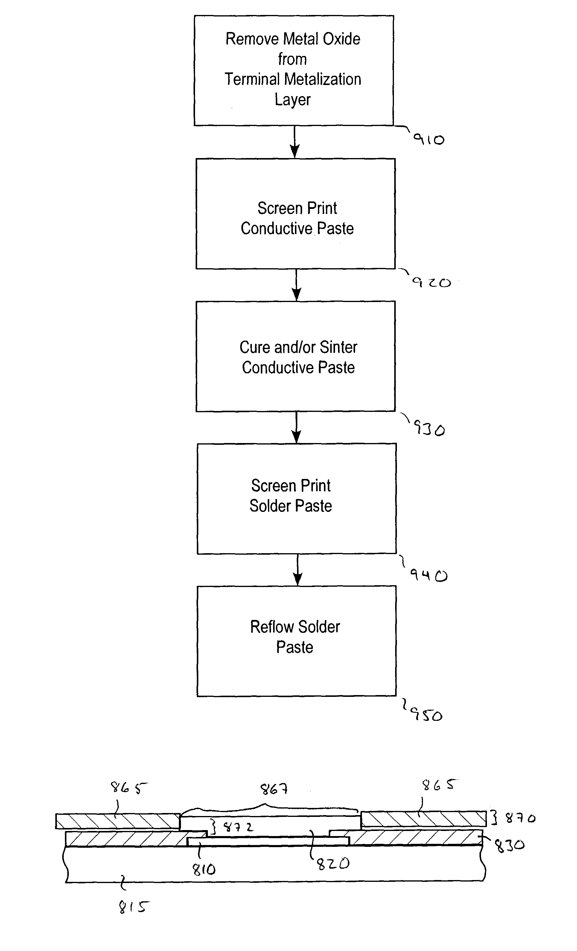
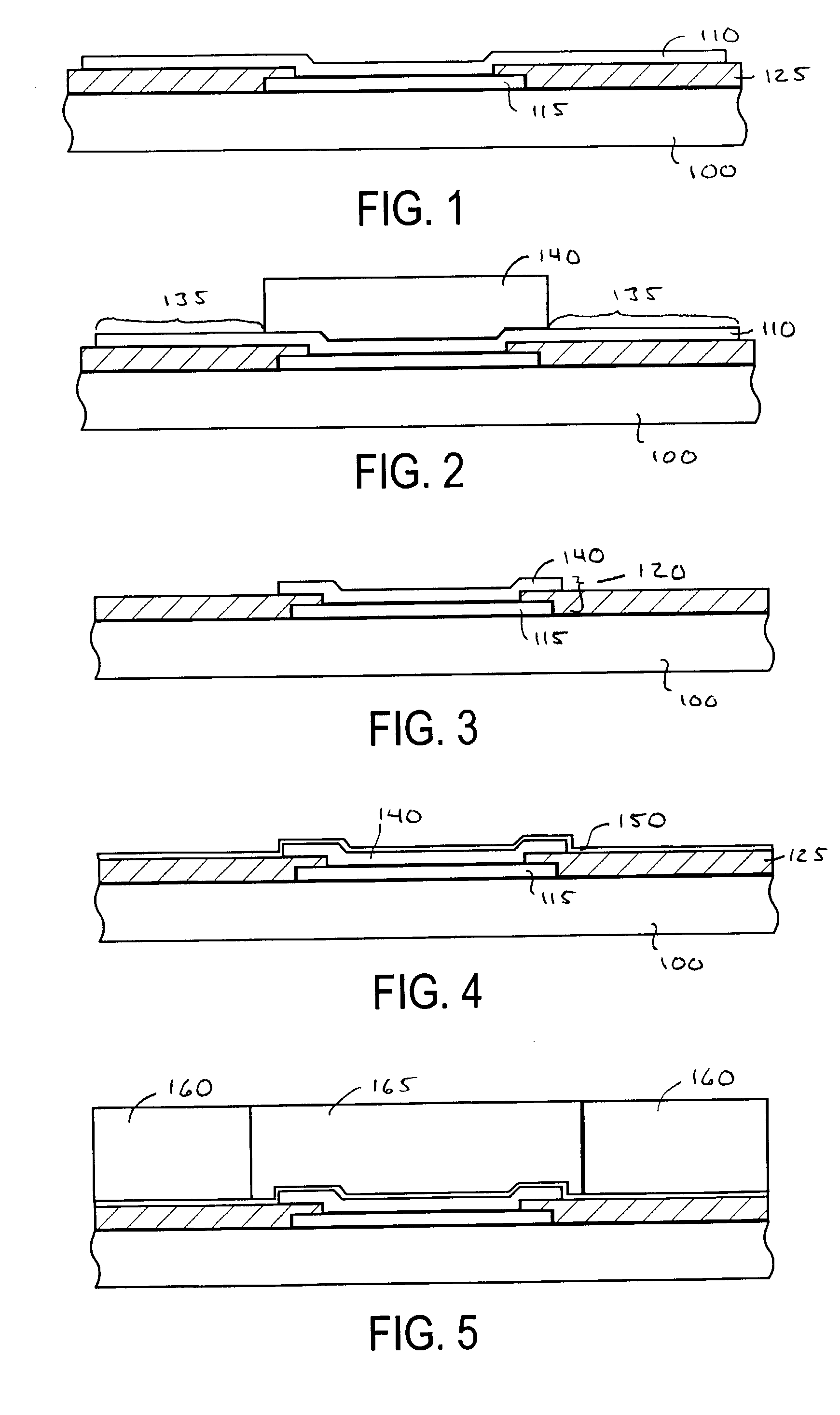
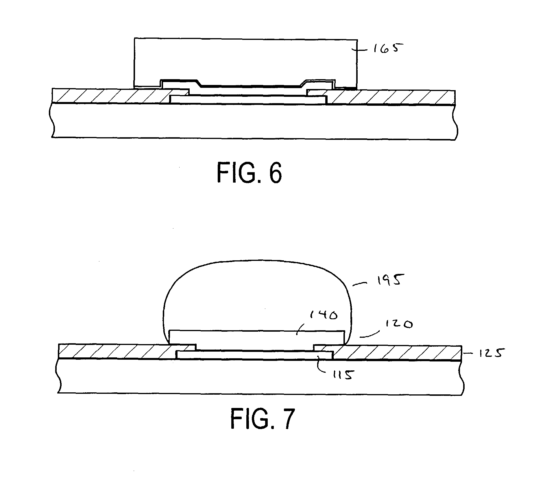
[0020]Embodiments of the present invention are directed toward methods for forming a conductive layer of an interconnect pad on an integrated circuit using screen printing techniques. Unlike known techniques, such as sputtering techniques, the method of the present invention does not engender the problems of sputtering, such as relatively high cost and lengthy processing times.

[0021]Screen printing techniques have been widely used in the graphic arts fields to produce art work and have found use in the production of printed circuit boards to transfer relatively large scale mask patterns onto printed circuit boards. Screen printing techniques include the use of a stencil to selectively transfer an image onto a substrate. The image is typically transferred by mechanically pressing a given material through porous (e.g., mesh) portions of the stencil onto a substrate while adjacent non-porous portions of the stencil do not permit printing of the material. Screen printed materials of use...


PUM


Abstract

A method for forming an integrated circuit interconnect pad is described. In one embodiment a method of forming an integrated circuit comprises screen printing a conductive paste onto a terminal metalization pad and curing the conductive paste in an inert or reducing atmosphere at an elevated temperature to form an under-bump metalization layer of an interconnect pad. The elevated temperature is below a melting temperature of the terminal metalization pad.

Description

BACKGROUND OF THE INVENTION[0001]The present invention relates to integrated circuit fabrication and to the formation of interconnect pads on an integrated circuit device. Specific embodiments of the invention relate to a method for forming an interconnect pad having a screen printed conductive layer. Methods of the present invention are of use in forming a screen printed conductive layer on a variety of integrated circuit metal pads, such as copper, aluminum, and gold pads among others.[0002]The semiconductor industry continues to produce integrated circuits (ICs) of increasing complexity and increasing density. The increased complexity of some of these integrated circuits has in turn resulted in an increased number of interconnect pads on the circuit chips. Each pad can be used for conventional wire bonding or flip chip bonding. At the same time, the increased density of the chips has driven the interconnect pad pitch downward. The combination of these two trends has been a signif...

Claims


Application Information

Patent Timeline
Patent Type & Authority Patents(United States)
IPC IPC(8): H01L21/44H01LH01L21/60
CPCH01L24/11H01L2224/13006H01L2224/13099H01L2924/01004H01L2924/01012H01L2924/01013H01L2924/01016H01L2924/01022H01L2924/01027H01L2924/01029H01L2924/0103H01L2924/01046H01L2924/01057H01L2924/01078H01L2924/01079H01L2924/14H01L2924/01006H01L2924/01023H01L2924/01033H01L2924/014H01L2224/0401H01L2224/11334H01L2224/03505H01L24/03H01L24/05H01L2224/05124H01L2224/05144H01L2224/05147H01L2924/351H01L2924/00H01L2924/00014H01L2924/013
Inventor LIN, PAUL T.
Owner KULICKE & SOFFA IND INC
Why Eureka
Try Eureka