Methods for forming silicon dioxide layers on substrates using atomic layer deposition

Active Publication Date: 2006-01-31
SAMSUNG ELECTRONICS CO LTD
View PDF28 Cites 82 Cited by
  • Summary
  • Abstract
  • Description
  • Claims
  • Application Information

AI Technical Summary

Benefits of technology

[0011]Accordingly, a general object of this invention is to provide improved methods for using atomic layer deposition (ALD) to grow h

Problems solved by technology

As a result, a problem arises due to increased pattern density variation and a corresponding decrease in uniformity.
Klaus '442 teaches, however, that the big drawback to ALD techniques was that they typically required temperatures greater than 600° K. and reactant exposures of greater than 109 L (where 1 L=10−6 Torr see) for the surface reactions to reach completion.
Such high temperature and high exposure procedures are not desirable for ultra-thin film depo

Method used


Image

  • Methods for forming silicon dioxide layers on substrates using atomic layer deposition
  • Methods for forming silicon dioxide layers on substrates using atomic layer deposition
  • Methods for forming silicon dioxide layers on substrates using atomic layer deposition

Examples


first exemplary embodiment

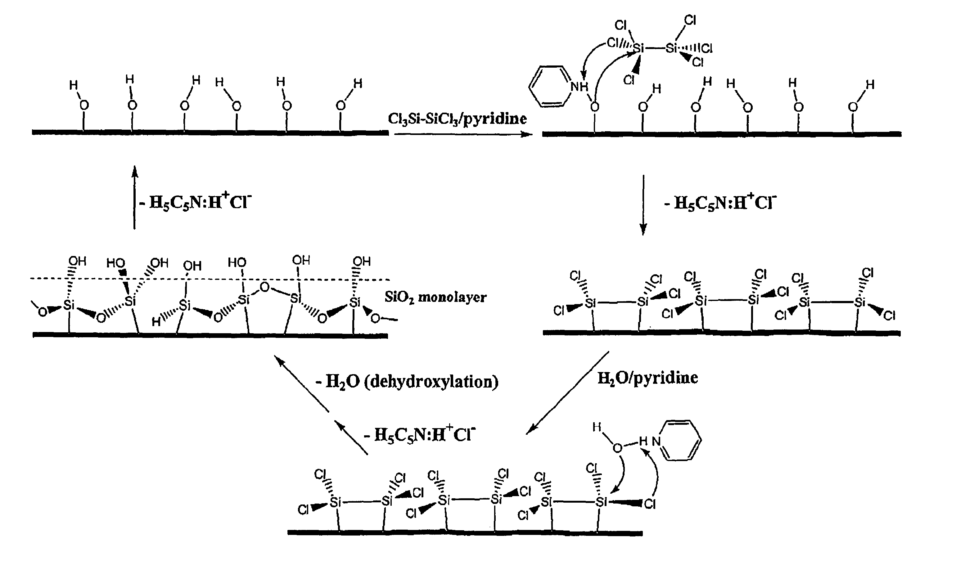
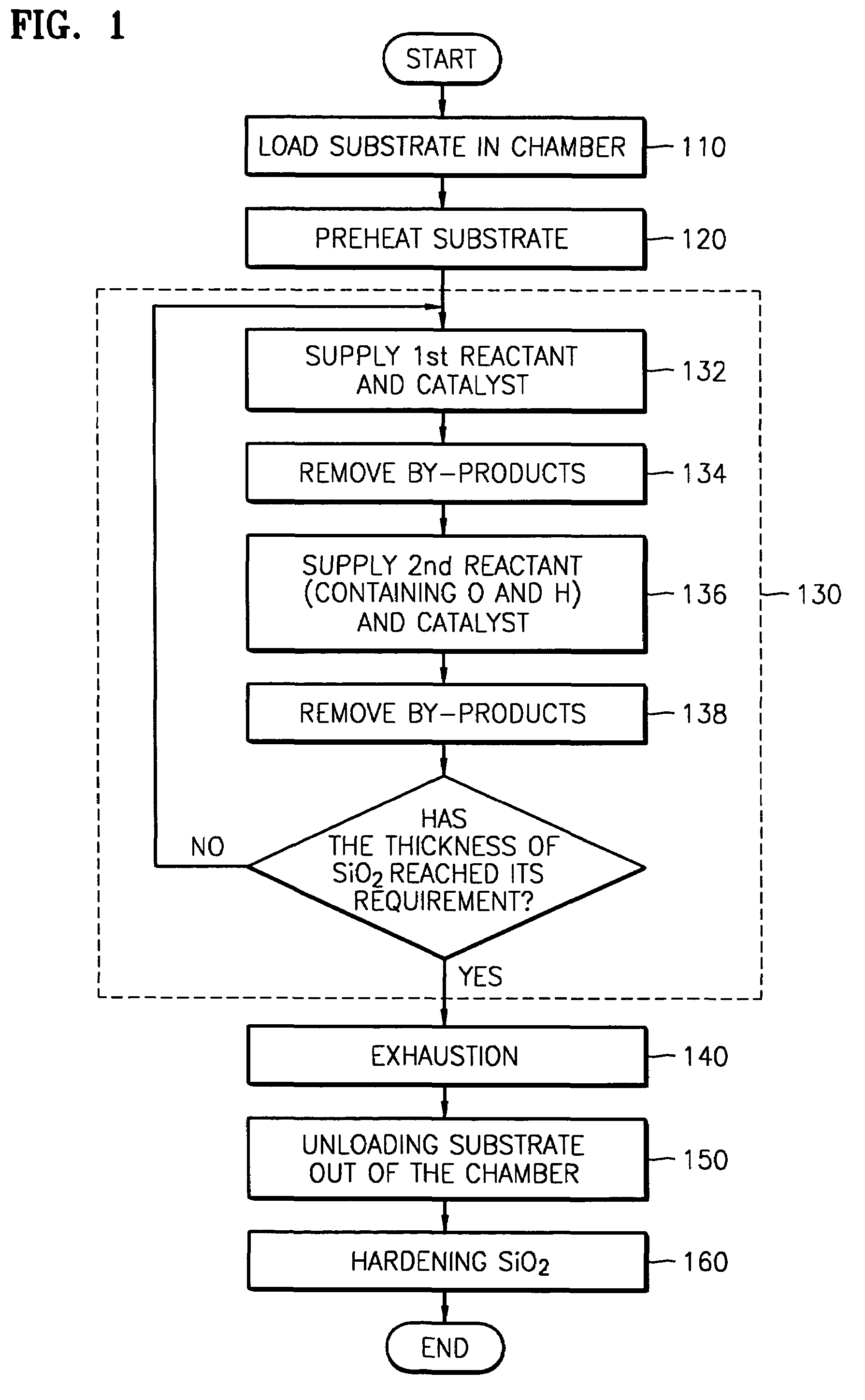
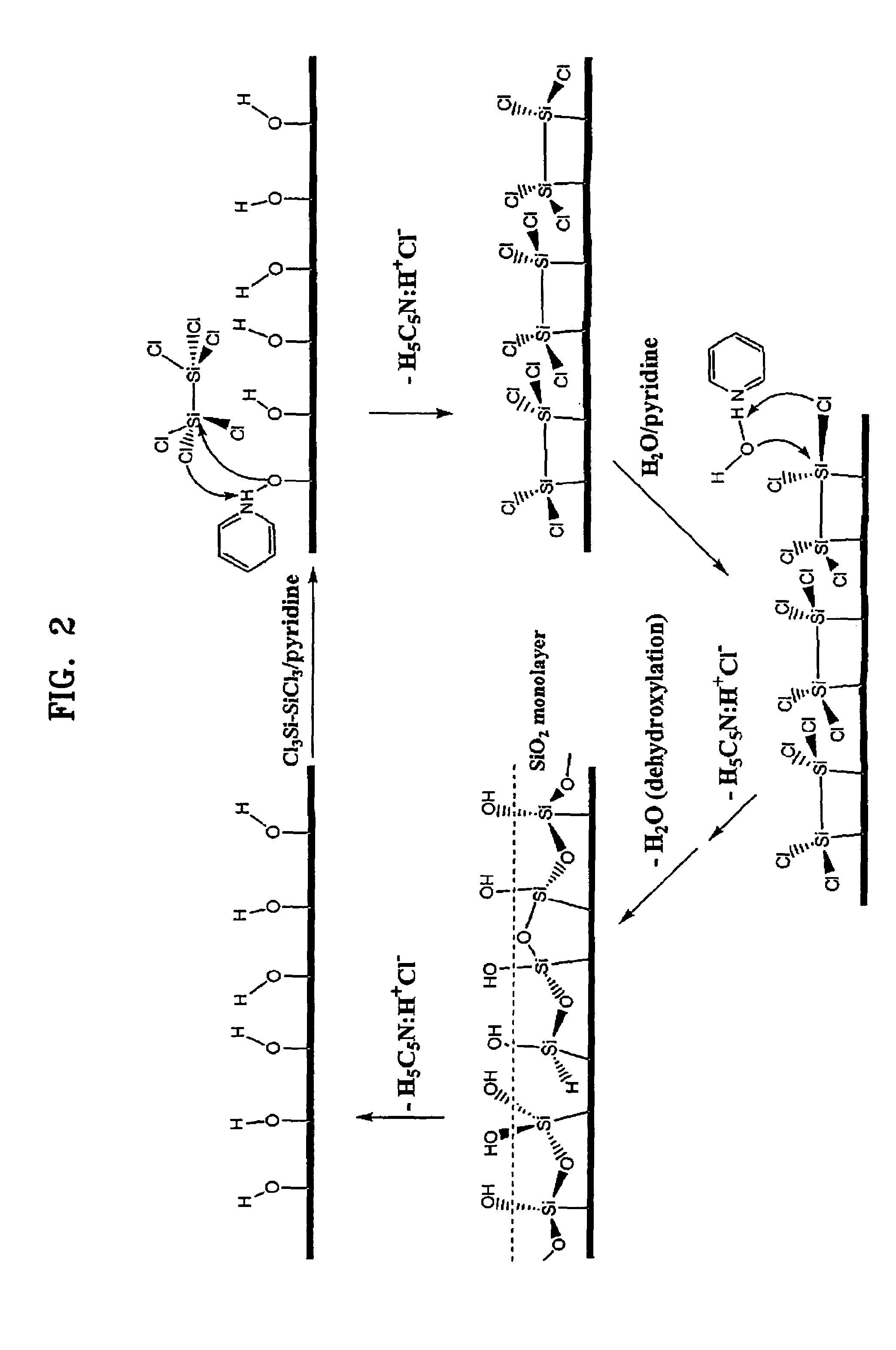
[0058]According to a first exemplary embodiment of the present invention, silicon dioxide thin films are grown on the functionalized surface of a substrate having hydroxyl groups using Si2Cl6 or a comparable compound, e.g., a silicon halide having two or more silicon atoms, as the first reactant; a compound containing O and H elements, e.g., H2O and / or H2O2, as the second reactant; and a base compound, e.g., ammonia or an amine, as the catalyst. For this embodiment of the invention, the first reactant is a silicon compound having at least two silicon atoms, for example a silicon-halide compound selected from the group consisting of: Si2X6, Si3X8, Si4X10, and Si3X6 (Triangle), which has the following chemical structure:

wherein X is a halogen such as F, Cl, Br, I. In a preferred embodiment, the first reactant is selected from the group consisting of Si2Cl6, Si3Cl8, Si4Cl10 and Si3Cl6(Triangle). For this embodiment of the invention, the second reactant is a compound containing oxygen ...

second exemplary embodiment

[0066]According to a second exemplary embodiment of this present invention, silicon dioxide thin films are grown on a functionalized surface of a substrate using a silicon halide as the first reactant; a second reactant containing O and H atoms, e.g., H2O and / or H2O2; and a tertiary aliphatic amine catalyst. In this embodiment of the invention, by exposing the functionalized surface of the substrate to a mixture of the first reactant and the catalyst in a first process step, a chemisorbed layer of the first reactant is formed along the substrate surface. Unreacted first reactant and byproducts are then removed from the region of the substrate. In the next process step, the chemisorbed layer of the first reactant is reacted with the second reactant in the presence of the tertiary aliphatic amine catalyst. Byproducts of this second reaction step are removed from the substrate region.

[0067]In accordance with this invention embodiment, it has been found that the use of a tertiary alipha...

third exemplary embodiment

[0076]According to a third particularly preferred embodiment of the present invention, many if not all of the advantages and benefits of both of the earlier-described embodiments of this invention can be realized. In this embodiment, silicon dioxide thin films are grown on a functionalized surface of a substrate using a silicon compound having at least two or more silicon atoms, e.g., a silicon halide such as Si2Cl6, as the first reactant; a compound containing O and H atoms, e.g., H2O and / or H2O2, as the second reactant; and, a tertiary aliphatic amine catalyst.

[0077]Thus, in accordance with this invention embodiment, the functionalized surface of the substrate is exposed to a mixture of the first reactant and the tertiary aliphatic amine catalyst in a first process step to form a chemisorbed layer of the first reactant along the substrate surface. Unreacted first reactant and any byproducts are then removed from the region of the substrate. In the next process step, the chemisorbe...


PUM

PropertyMeasurementUnit
Temperatureaaaaaaaaaa

Abstract

Improved methods are disclosed for catalyst-assisted atomic layer deposition (ALD) to form a silicon dioxide layer having superior properties on a semiconductor substrate by using a first reactant component consisting of a silicon compound having at least two silicon atoms, or using a tertiary aliphatic amine as the catalyst component, or both in combination, together with related purging methods and sequencing.

Description

BACKGROUND OF THE INVENTION[0001]1. Field of the Invention[0002]The present invention relates generally to improved methods for growing silicon dioxide layers on substrates, such as in semiconductor manufacture, using atomic layer deposition processes. The methods of this invention facilitate exercising extremely precise control over the properties of a silicon dioxide layer applied, for example, to a gate oxide or a dielectric layer. The methods of this invention have particular utility in fabricating gate spacers, gate oxides, silicide blocking layers, bit line spacers, inter-level dielectric layers, etch stoppers, and related final or intermediate products in semiconductor fabrication.[0003]2. Description of the Related Art[0004]In manufacturing a semiconductor device, a silicon dioxide layer is typically formed on a substrate surface by such conventional techniques as chemical vapor deposition (CVD), low-pressure CVD (LPCVD), or plasma-enhanced CVD (PECVD). These techniques are ...

Claims


Application Information

Patent Timeline
IPC IPC(8): H01L21/302H01L21/205C23C16/40C23C16/44C23C16/455H01L21/312H01L21/314H01L21/316H01L21/76
CPCC23C16/402C23C16/45534C23C16/56H01L21/02164H01L21/02208H01L21/31612H01L21/0228H01L21/02337H01L21/0234H01L21/3122H01L21/3141H01L21/02277H01L21/205
Inventor LEE, JOO-WONPARK, JAE-EUNYANG, JONG-HOCHU, KANG-SOO
Owner SAMSUNG ELECTRONICS CO LTD
Why Eureka
Try Eureka