Semiconductor device

Active Publication Date: 2006-01-31
SOCIONEXT INC
View PDF5 Cites 20 Cited by
  • Summary
  • Abstract
  • Description
  • Claims
  • Application Information

AI Technical Summary

Benefits of technology

[0034]In addition, according to the present invention, a pad portion of an electrode pad having the smallest width extends to reach the inside of the internal circuit. Thus, when the electrode pad is used as a power supply pad, a voltage drop caused in supplying a supply voltage can be effectively reduced. Therefore, a favorable power supply becomes possible.
[0035]Moreover, according to the present invention, in a cell, a line which is connected to an electrode and provided in an uppermost layer is provided at a predetermined distance from an end portion of the cell in the inward direction. Thus, even

Problems solved by technology

However, when the above-described multi-stepped structure is used for an electrode pad, the fo

Method used


Image

  • Semiconductor device
  • Semiconductor device
  • Semiconductor device

Examples


first embodiment

[0050

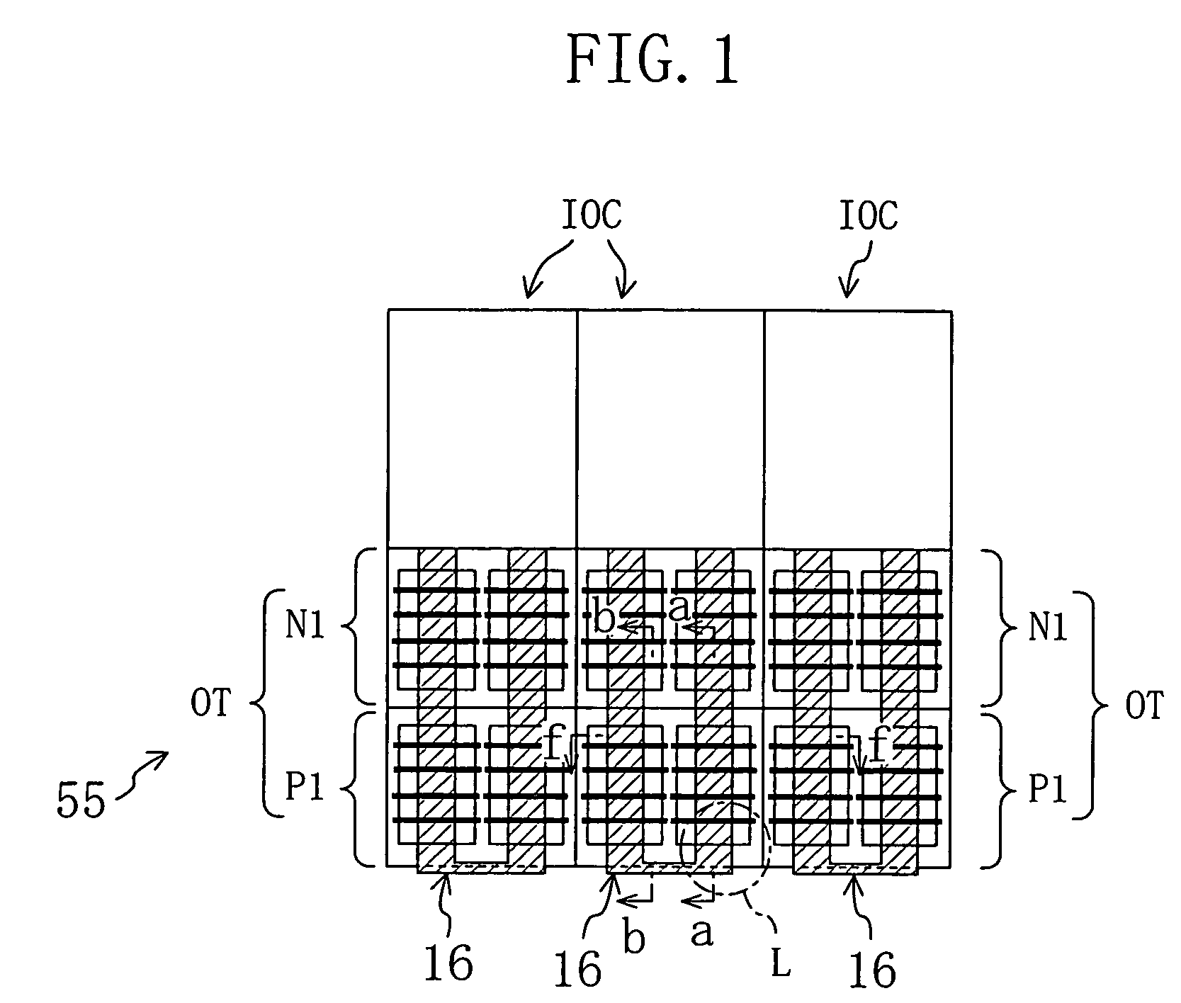
[0051]FIG. 1 is a plan view illustrating a specific arrangement of a semiconductor device according to a first embodiment of the present invention.

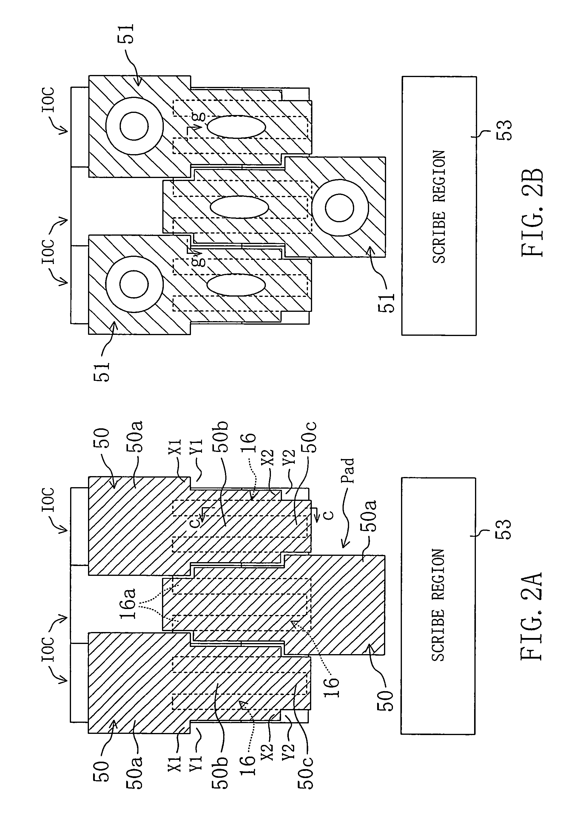
[0052]FIG. 1 shows the arrangement of major part of an I / O circuit unit provided in the periphery of a semiconductor chip, in which a plurality (e.g., three in FIG. 1) I / O cells IOC are arranged in lines. FIGS. 2A and 2B are views illustrating an arrangement in which an electrode pad cell is provided over each of the three I / O cells IOC.

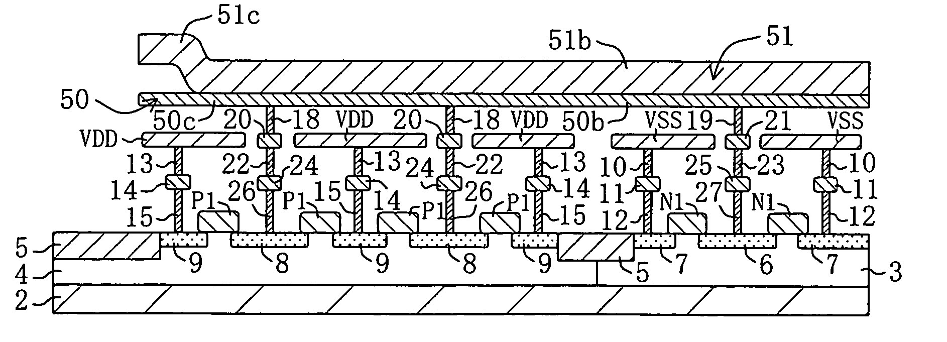
[0053]First, the structure of each of the I / O cells IOC will be described. FIG. 3A is a cross-sectional view taken along the line a-a shown in FIG. 1. FIG. 3B is a cross-sectional view taken along the line b—b shown in FIG. 1. In FIGS. 3A and 3B, 2 denotes a p-type semiconductor substrate, 3 and 4 denote p-type and n-type wells formed on the semiconductor substrate 2, respectively. Four separate NMOS transistors N1 are provided on the p-type well 3, and four separate PMOS transistors P1 are provided o...

second embodiment

[0070

[0071]Hereinafter, a second embodiment of the present invention will be described with reference to FIGS. 6A through 6C.

[0072]In this embodiment, an electrode pad cell is used as a power supply terminal cell. In FIG. 6A, an I / O cell IOC′ has a structure in which each of end portions of a U shaped connection line 16′ provided in an uppermost layer widely extends toward an internal circuit provided in a semiconductor chip (located in an upper portion in the structure of FIG. 6A, but not shown).

[0073]Moreover, in FIG. 6B, the electrode pad cell Pad′ has a structure in which the third pad portion 50c of a lower electrode pad (power terminal pad) 50′ which contains part of the connection line 16′ and has the smallest width or the first pad portion 50a′ of the lower electrode pad 50′ extends toward the inner circuit. An upper electrode pad 51′ shown in FIG. 6C has the same structure as that of the lower electrode pad 50′ in which counterparts of the first pad portion 50a′ or the thir...


PUM


Abstract

In an I/O circuit unit located in the periphery of a semiconductor chip, a plurality of ESD protection transistors are provided in each I/O cell. An electrode pad cell has a two-layer structure including a lower electrode pad and an upper electrode pad. The electrode pad cell is arranged so as to be present over a connection line of ESD protection transistors of an associated I/O cell. With part of the first pad portion of an adjacent electrode pad located in an end portion of the second pad portion of the electrode pad, the second pad portion can not extend further onward but the third pad portion having a smaller width than that of the second pad portion is arranged onward. Thus, destruction of the ESD protection transistors is not caused, so that an internal circuit is protected from an electrostatic discharge which comes into electrode pads.

Description

BACKGROUND OF THE INVENTION[0001]The present invention relates to semiconductor devices and more particularly relates to improvement of an I / O circuit unit including an output transistor for transmitting an output of an internal circuit to the outside and a protection transistor for protecting the internal circuit from an electrostatic discharge (ESD) from the outside.[0002]In a semiconductor integrated circuit, generally, an I / O circuit unit for performing input / output between the outside and an internal circuit is provided in the periphery of a semiconductor chip and the I / O circuit unit includes a plurality of electrode pads. Hereinafter, the structure of a known I / O circuit unit will be described.[0003]FIG. 7 is a circuit diagram of a known I / O circuit unit. In FIG. 7, P101 denotes a p-type MOS transistor, and the source thereof is connected to a power line VDD. N101 denotes an n-type MOS transistor, and the source thereof is connected to a ground line VSS. The respective drains...

Claims


Application Information

Patent Timeline
IPC IPC(8): H01L23/62H01L21/82H01L27/04H01L21/822H01L23/485H01L23/528H01L23/544H01L23/60H01L27/02
CPCH01L22/32H01L22/34H01L24/06H01L27/0251H01L2924/13091H01L2924/01005H01L2924/3011H01L23/5286H01L24/02H01L2224/05624H01L2224/4943H01L2924/01004H01L2924/01006H01L2924/01013H01L2924/01029H01L2924/01033H01L2924/01082H01L2924/14H01L2924/00014H01L2924/00H01L2224/05552
Inventor TANIGUCHI, KOICHINOJIRI, NAOKI
Owner SOCIONEXT INC
Why Eureka
Try Eureka