
Projection optical system
a technology of which is applied in the field of projection exposure apparatus, can solve the problems limited number of suitable materials for lenses in projection optical system and illumination optical system having a large enough transmittance at short wavelengths, and inability to achieve the effect of reducing the problem of deterioration of optical performan
- Summary
- Abstract
- Description
- Claims
- Application Information
AI Technical Summary
Benefits of technology
Problems solved by technology
Method used
Image

Examples
Embodiment Construction
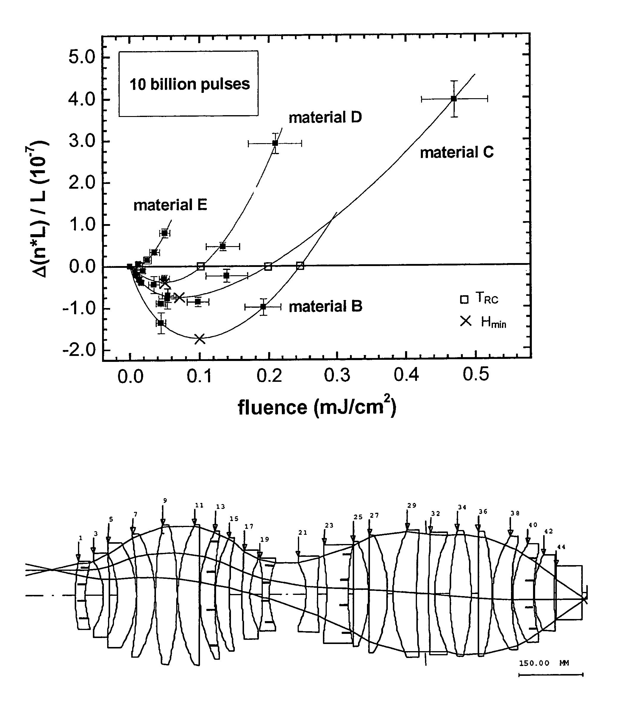
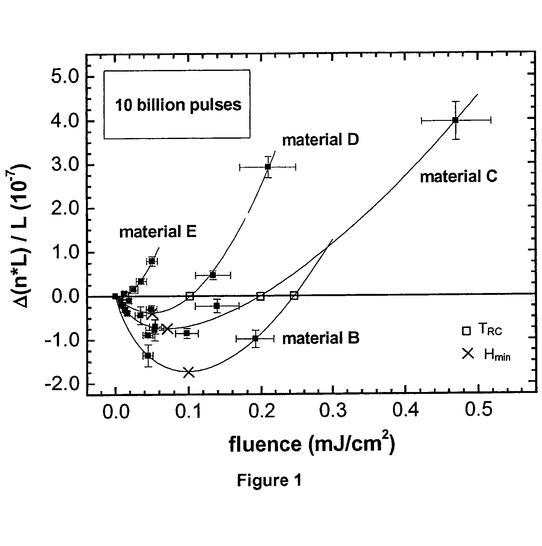
[0121]FIG. 1 illustrates results from experiments in which 10 cm long samples of lens materials B to E were each exposed to 10 billion pulses of radiation having fluence values in the range of 0.01 to 0.5 mJ / cm2. The relative optical path length difference Δ(n·L) / L of the respective sample is plotted against the fluence value that the respective sample of the lens material was exposed to. The light source used was an ArF excimer laser emitting light of 193 nm wavelength (λ). The pulse length (more precisely: integral square pulse width) was about 25 ns. The relative optical path length difference Δ(n·L) / L was measured using an interferometric method (using light of 633 nm wavelength).
[0122]As can be clearly seen in FIG. 1, each lens material shows a characteristic dependency of the change in physical properties on the exposure fluence value.
[0123]Each lens material can be characterised by a characteristic transition point (TRC) which marks the fluence value upon radiation to which t...
PUM
| Property | Measurement | Unit |
|---|---|---|
| wavelength | aaaaa | aaaaa |
| wavelengths | aaaaa | aaaaa |
| wavelengths | aaaaa | aaaaa |
Abstract
Description
Claims
Application Information